 Tony Finch – blog
I’m a beginner at PCB design, or rather, I haven’t made a PCB since I was at school 30 years ago, and a lot has changed since then! So my aim for Keybird69’s PCB was to learn my way around the design, manufacturing, and assembly process.
microcontroller
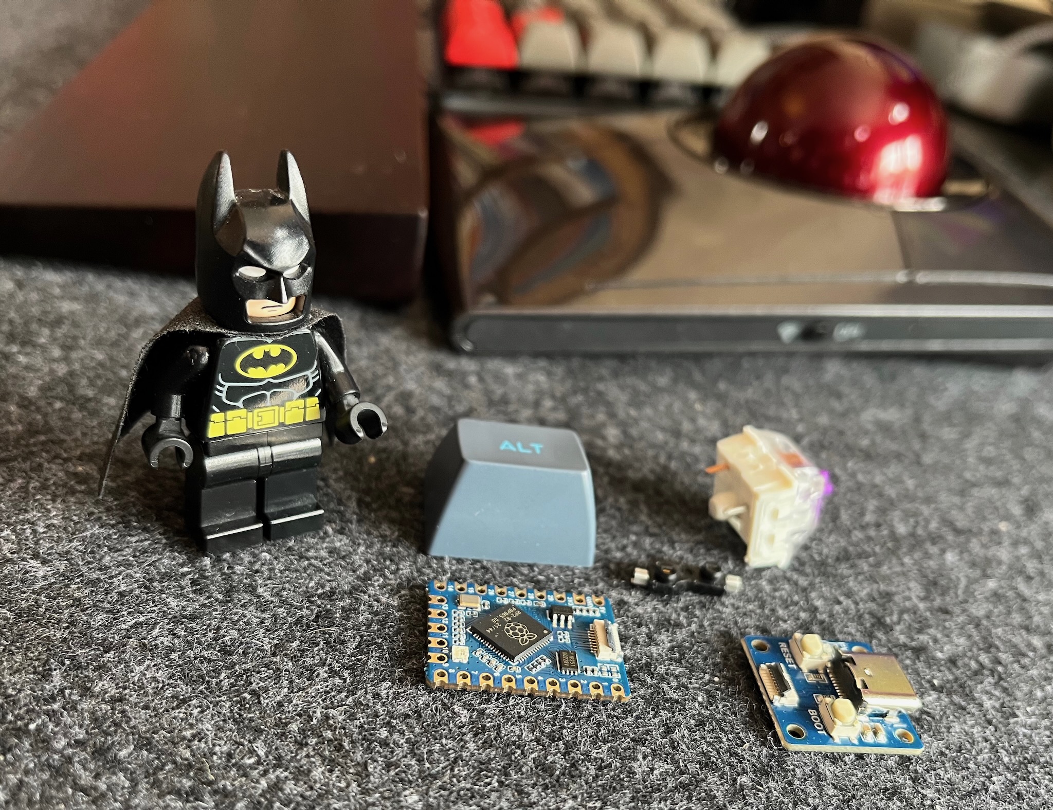
To avoid all the difficult parts of the PCB design, I used the Waveshare RP2040-Tiny. This is, basically, a Raspberry Pi Pico that has been split in two. There are some other differences: USB-C instead of micro-USB, a reset button, fewer GPIO pins broken out to the board edge.
The RP2040-Tiny microcontroller board is about the size of an ALT keycap, so it easily fits under the space bar. The USB-C board is smaller, tho I would have preferred it to be wider and shallower.
other components
Apart from the controller, all that is needed is a switch and a diode for each key.
Because this keyboard is experimental, I wanted the switches to be socketed, using Kailh MX hotswap sockets. This makes it possible to change switches without desoldering them (I am trying out different switches for my modifier keys) but it also makes it possible separate the switch mounting plate from the PCB to fettle the stabilizers or add/remove sound damping foam.
My plan was to get the PCBs manufactured with diodes and sockets already soldered on, but that did not quite work out - about which more below.
key matrix
A keyboard matrix has some row wires and some column wires; each switch connects a row and a column, via a diode that allows the controller to disambiguate when multiple keys are pressed at the same time. The row and column wires are connected to the microcontroller GPIO pins.
Normally the rows and column wires correspond fairly directly to the visible layout of the keyboard, but for some reason I decided to use ai03’s duplex matrix design where one row of keys has two row wires, and two columns of keys use the same column wire.
So the Keybird69 matrix is 8 x 9, using 17 GPIO pins, where a more normal layout would be 16 x 5 using 21 GPIO pins. (The RP2040-Tiny has more than enough GPIOs for a normal matrix, so there was no need for me to use the fancy duplex matrix.)
firmware
There are a few options for keyboard firmware:
- QMK seems to be have the most momentum behind it
- KMK is for the Pythonistas
- ZMK has less historical baggage than QMK
I got QMK working on the Waveshare RP2040-Tiny without too much difficulty.
I can configure QMK with just its data-driven JSON configuration,
without needing any C – the differences from the GENERIC_RP_RP2040
platform are minimal.
I also got QMK working on my Pimoroni Keybow 2040.
Amusingly (in retrospect) I found it more difficult to get the LEDs working than the keyboard matrix scanner – I expected board bringup to involve blinking an LED first, before moving on to more complicated things. But it turns out that there’s a lot more complexity around keyboard LEDs than scanning a keyboard matrix, both from the hardware and firmware points of view. (See the Keybow 2040 pull request for some of my frustrations.)
To test the firmware, I plugged the bare microcontroller board into my computer and used a wire to connect pairs of GPIO pins. This made it generate the right USB HID events, so I could use it like a really super awkward keyboard.
design
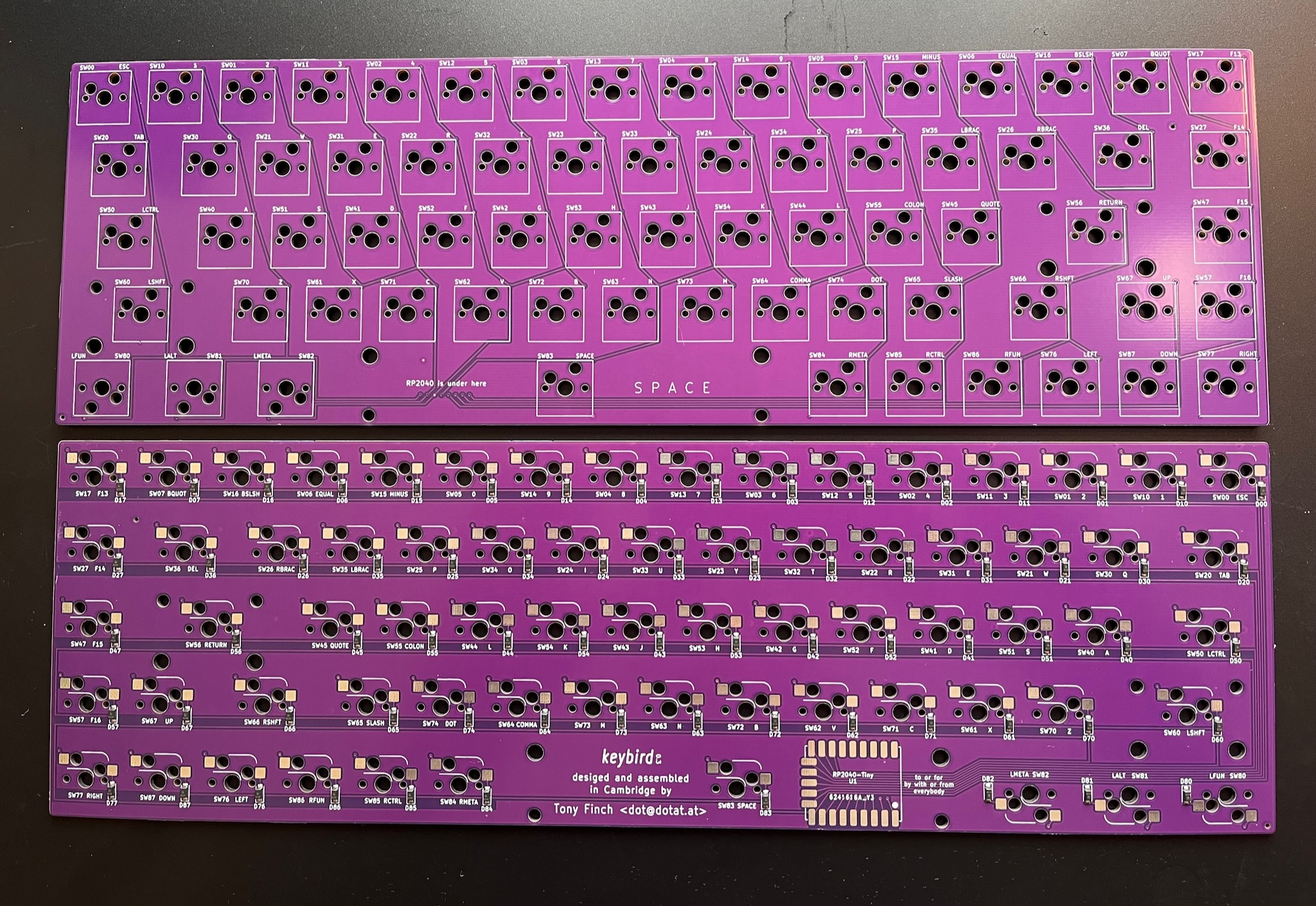
This picture comes out a lot paler and redder than it appears in the flesh: in reality the PCB has a deeper imperial purple lustre.
I generally followed Ruiqi Mao’s keyboard PCB design guide and ai03’s keyboard PCB design guide.
They are both helpful guides to KiCad’s preferred workflow of drawing up the schematic first, then turning the abstract diagram into a physical PCB layout.
I like being able to reconcile the schematic and the PCB in both directions, so when I found the layout would work better with a different assignment of row and column wires to GPIO pins, KiCad would warn me when things were inconsistent. I felt reassured that it was helping me to avoid mistakes.
I had a bit of fun with the duplex matrix: Each row has a pair of PCB tracks running across the bottom of the board; I left out the ground plane fill between the row tracks, so they appear as much darker stripes on the PCB. (This is probably horrible for EMI?) Each switch’s diode bridges over one of the row tracks, so the diode’s cathode can connect to either of the row tracks without extra faff.
The bottom-right modifier keys are rotated to make extra space for the bus (labelled “to or for by with or from everybody”) that connects the microcontroller tp the rows.
plates
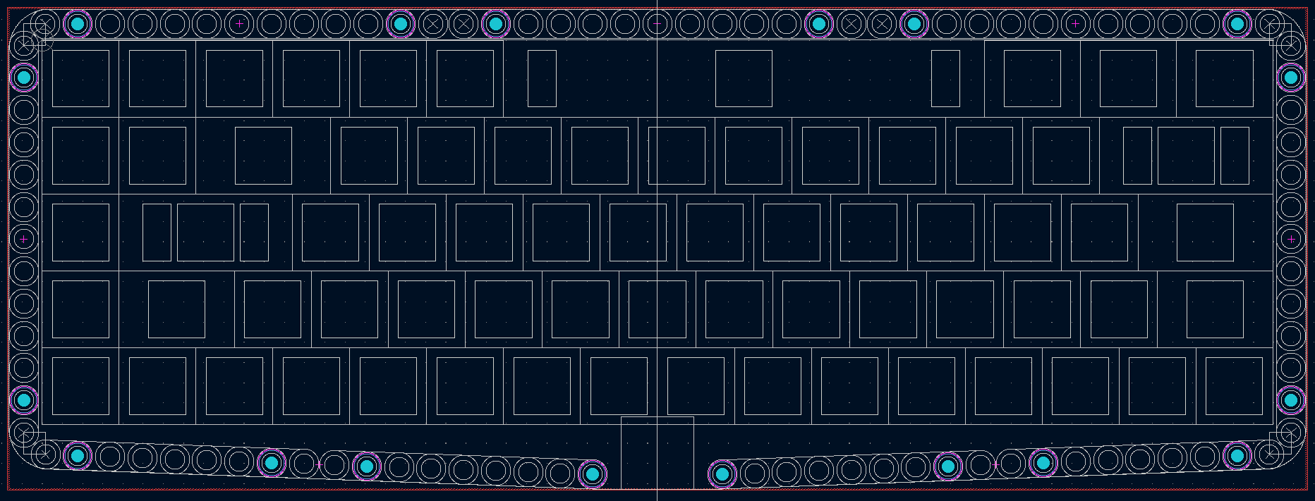
I also used KiCad to design the switch mounting plate and the base plate for the case.
I made some custom footprints for the LEGO Technic beams, which were mostly outlines on the “user comments” layer. Along with some scaffolding to fix the geometry of the corners, the beams indicated where the plate outlines and fastening holes needed to be.
This made it easier to get everything into the right place than it was for the PCB. The constraints imposed by using LEGO were helpful.
I had some trouble with the cutouts for the stabilizers that keep the long keys (space, return, etc.) level. The Cherry MX data sheet, ai03’s plate tool, the swillkb plate tool, and measurements of actual stabilizer housings all disagreed with each other. It does not help that the measurements use a ridiculous mixture of inches and millimetres. I chose a cutout size that I thought should fit, using round numbers of millimetres (Cherry is a German company).
I was not sure what to do about kerf, the difference between the tooling path and the edge of the cut. The tolerances specified in the Cherry MX data sheet are much finer than JLCPCB’s manufacturing tolerances, so I simply drew the switch cutouts as 14mm squares and hoped that would be good enough.
manufacturing
I got the boards made by JLCPCB, who are impressively cheap and fast. (Though a keyboard PCB is larger than the 100mm x 100mm limit for their super-cheap tier.)
When you submit an order, the JLCPCB web site shows you a picture of the board so you can do some final verification. I was worried by a bug: it does not render holes that are described in the board edge cuts layer, so my switch mounting plate was drawn without the holes for the switches. I found some forum conversations discussing this issue, saying that their boards were made correctly despite the rendering bug.
There were questions from the JLCPCB engineering staff about whether the mounting holes for the keyswitches were supposed to be plated or not, which caused a few days of delay. Once we were past that, I was impressed by JLCPCB’s live manufacturing progress tracker.
Another thing I found difficult about the submitting the order to JLCPCB was understanding what is part of their “Economic PCBA” offer.
One aspect is choice of components: JLCPCB has a huge parts library which has three important levels of classification:
-
“basic parts” are pre-loaded onto the pick-and-place machines, so you only pay the per-part cost;
-
“extended parts” have to be manually loaded, so there’s a fee for each different extended part you use;
-
there are also “standard only” parts which are not available for “Economic PCBA”
For my PCB, the Kailh hotswap sockets are “standard only” which meant it was better for me to obtain them elsewhere and solder them on myself. So the only soldering JLCPCB did for me was the diodes.
For a while I was also worried about the design-for-manufacturing requirements for panelization (how multiple PCBs are assembled as part of as single large sheet), fiducials (optical markers used by pick-and-place machines for precise positioning), tooling holes (for mounting the board in various machines). Eventually I worked out that for Economic PCBA, JLCPCB will take care of all of these details.
(Their documentation is excellent, but not always clear which flavour of PCB asembly is relevant for a particular requirement.)
An amusing thing I found when browsing the parts library is the term “brick nogging” which is apparently a mistranslation of an abbreviation for “vertical surface mount”. This came up when I was investigating options for USB-C sockets that occupy less vertical space. One of the options is “mid-mount” where the socket is recessed into the PCB; the JLCPCB parts library gives this the evocative name “sink board”.
assembly
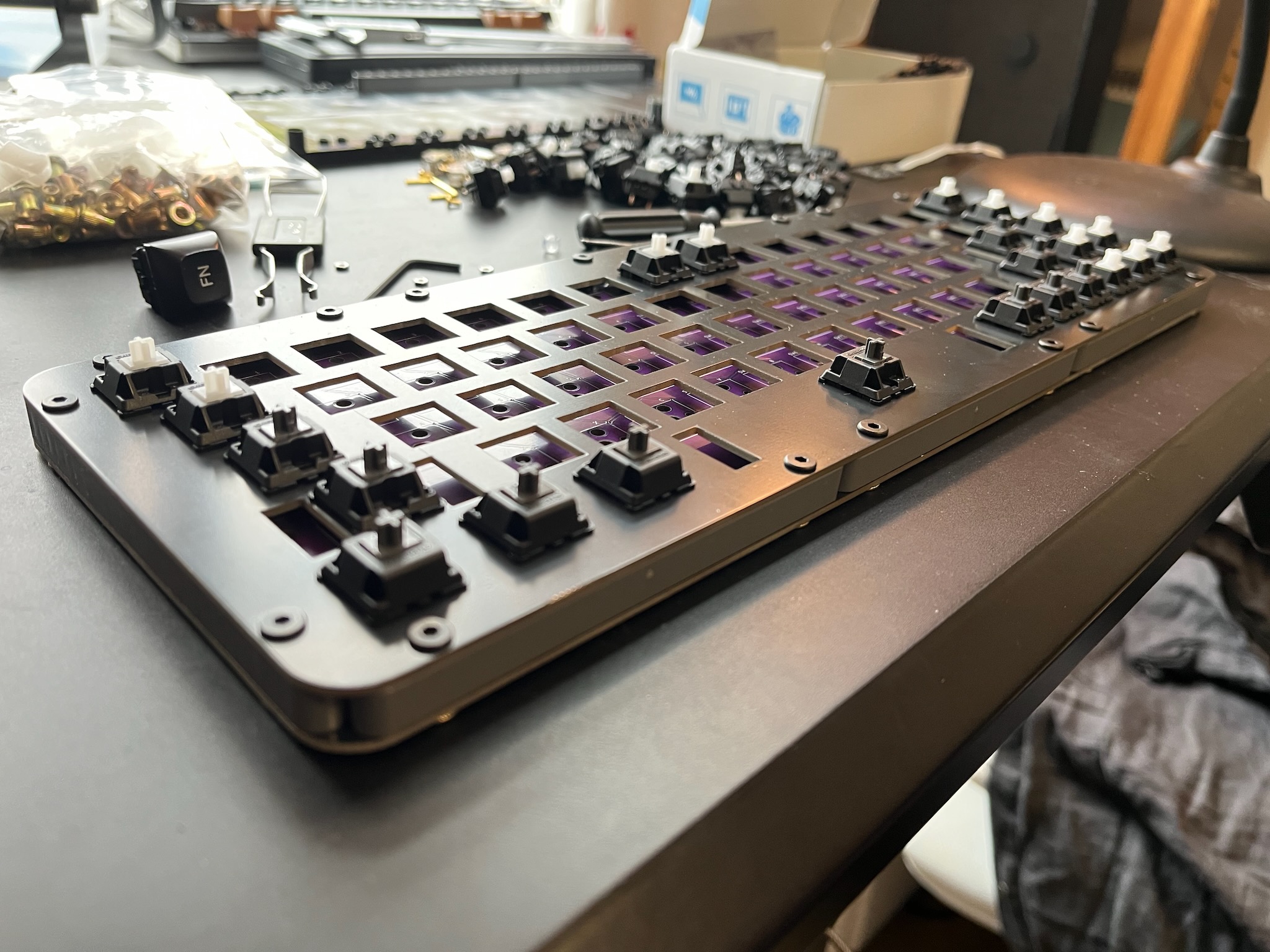
When the boards arrived, I started by checking that mechanical assembly would work. Happily the stabilizers and switches fit very nicely into their cutouts in the top plate.
There was a worrying moment when I expected the switches to fit into the PCB easily, but they didn’t. It turned out that the mounting holes are very snug, and the switches need a little force to make them fit. (I thought the insertion force in my HHKBeeb came from the hotswap sockets; turns out it isn’t just the sockets.)
After I got past that, everything fitted together perfectly. I was hugely relieved.
Then I started attaching the microcontroller. After some fumbling attempts with my old plug-in-get-hot soldering iron, I decided I would need something with a finer tip.
I had heard that the Pine64 Pinecil is a reasonably effective and inexpensive soldering iron; bonus points for being open hardware designed to be hackable. Amazingly there is open source firmware for soldering irons called IronOS that works on the Pinecil and a number of other irons. Much credit is due to Miniware for making the TS100 soldering iron open enough to establish this niche. Soldering irons are now my second example (after mechanical keyboards) of how amazing open hardware and open firmware can be.
After soldering on the controller, I checked the switch matrix worked by plugging it into my computer and using tweezers to connect the pads for each hotswap socket. Everything worked!
Then I soldered on the keyswitch sockets. A meditative process. Except that lead-free solder is vexingly difficult to use.
To help my middle-aged eyes I used a 5x magnifying glass, 9cm diameter, mounted with a flexible neck on a desk stand like a lamp. I learned recently that magnifiers have an odd damping effect with the hand-eye coordination feedback loop that makes your hands more steady.
I also used some smaller more powerful lenses for visual inspection. There were a few badly soldered joints, and one where I was surprised that one of the metal connectors had pinged out of its socket without me noticing. Fortunately it was easy enough to find and solder it back where it should be.
After that, another test, and everything still worked! Amazing!