Long-awaited improvements in photolithography could pave the way for the continued shrinking and scaling of microprocessors into the second half of this decade and beyond.
Moore's Law—which says that transistor densities double every 18 to 24 months or so—is not some inevitable consequence of physics. Rather, it's an observation of the way the semiconductor industry has evolved: the investment and technological progress that companies like Intel have made results in an approximate doubling of transistor densities on a regular basis.
Rather than causing the doubling, physics is currently threatening to put an end to the progress we've seen over the last four decades. Microchips are made with a process called photolithography. The silicon wafer on which the chip is built is coated with a light-sensitive layer ("photoresist"). Light is then shone through a patterned mask onto the wafer, essentially burning away the photoresist in the exposed areas. This exposes some parts of the wafer, leaving others covered. The exposed parts are then etched away, and the remaining photoresist washed off.
The limiting factor is the size of pattern that can be created on the photoresist layer. Higher transistor densities require finer mask patterns and shorter light wavelengths. Here's the pressing issue: current photolithography uses ultraviolet light with a 193nm wavelength, but at some point in the near future, probably around the 10nm process, a switch to extreme UV (EUV) with a 13.5nm wavelength will be required.
In the late 1990s and early 2000s, there was confidence within the semiconductor industry that EUV equipment was coming soon. It has failed to materialize, however, due to the technical difficulties that EUV imposes. Optically, EUV is harder to work with. It precludes the use of lenses, as most optical materials strongly absorb EUV light. Instead only mirrors can be used.
Further, it's hard to generate EUV light. Two methods are used: discharge production passes a large current through a metal plasma or laser production heats droplets of tin with a high intensity laser beam. Neither method is very energy-efficient.
But good news could be on the horizon. ASML, the world's largest supplier of photolithographic equipment, has said (via HotHardware) that it could have production-ready commercial equipment by 2015, suitable for producing chips with 10nm features.
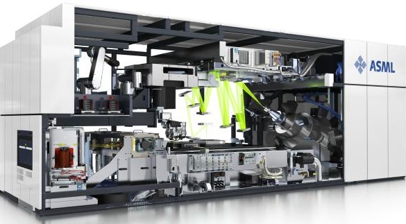
However, the company still has work to do to meet that goal. Its current prototype machine, using lasers to produce the EUV, produces about 55W of light. Commercial hardware will need to produce about 250W of light. (As if to highlight the difficulties that EUV has faced, ASML once expected to have 80W machines by the end of 2011.) Intel says that it needs 1kW light sources for its lithographic needs.
The problems with EUV photolithography could derail Moore's Law. Although there are workarounds that extend regular UV photolithographic techniques, such as using multiple exposures with different masks, these have challenges of their own (due to the tight alignment requirements of the different masks). The more masks and exposures used, the higher the chance of a misalignment ruining the wafer.
Current fabrication uses double patterning with two exposures. In the event that EUV hardware can't reach the power levels required, quadruple patterning is the next step, even with its attendant difficulties.
Listing image by Intel
reader comments
145