AMD Announces 64-Core 7nm Rome CPUs, 7nm MI60 GPUs, and Zen 4
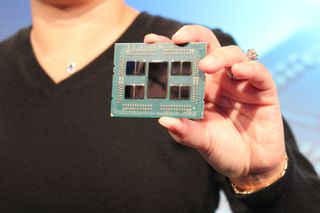
We're here at AMD's Next Horizon Event to bring you up to the minute news on the company's 7nm products. This is breaking news, so check back frequently or refresh the page for updates.
AMD is expected to make major announcements about its new 7nm CPUs and GPUs. Intel continues to struggle with its 10nm manufacturing process, which is delayed until late 2019. If AMD can field 7nm processors early next year, it will mark the first time in the company's history that it has had a process node leadership position over Intel. That should equate to faster, denser, and less power-hungry processors than Intel's 14nm chips.

AMD CEO Lisa Su is delivering the opening statements. She recounted the path of the EPYC data center processors to market and discussed many of the key roles those processors are used for, such as workloads in HPC, cloud, hyperscale, and virtualization environments. AMD sees the data center as a $29 billion opportunity by 2021, and GPUs are playing a larger role as the industry shifts to artificial intelligence and machine learning workloads.
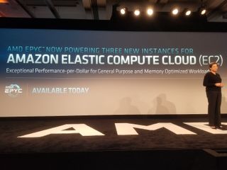
Amazon Web Services, one of the world's largest cloud service providers, announced that, beginning today, it is offering new EPYC-powered cloud instances. The R5a, M5a and T3a instances purportedly will offer a 10% price-to-performance advantage over AWS's other cloud instances.


Mark Papermaster will cover the new Zen 2 cores and AMD's 7nm process technology. AMD will also reveal more about the 7nm Mi60 Instinct GPU for the data center. AMD will also provide early specifications for AMD's Rome, the first x86 7nm processor for the data center.
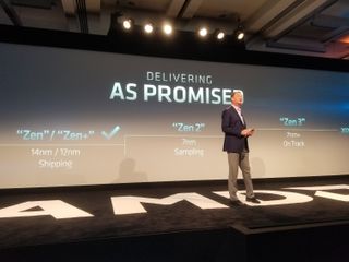
AMD is already sampling its 7nm Rome processors, which mark the debut of the Zen 2 microarchitecture, to customers. The firm also has its Zen 3 processors under development. This third-gen microarchitecture will debut on the 7nm+ process, with the "+" indicating this will be a second generation of the 7nm node (a "tock" equivalent).


The new processors feature faster, smaller, and lower-power transistors. As with all new nodes, development requires a significant investment from both AMD and TSMC, which will fab the parts. The high up-front costs associated with developing a new node pushed AMD's primary manufacturing partner, Global Foundries, out of the 7nm race earlier this year. AMD remains committed to delivering the new node and using it as a vehicle to deliver the new Zen 2 microarchitecture to market.
Stay on the Cutting Edge
Join the experts who read Tom's Hardware for the inside track on enthusiast PC tech news — and have for over 25 years. We'll send breaking news and in-depth reviews of CPUs, GPUs, AI, maker hardware and more straight to your inbox.
AMD also announced that it is already working on the Zen 4 microarchitecture, but didn't reveal significant details.


Zen 2 will provide up to 2X the compute power per node, improved execution pipeline, doubled core density, and use half the energy per operation. AMD has doubled floating point performance with the Zen 2 microarchitecture.


AMD has improved the branch predictor, pre-fetching engine, and doubled the load/store bandwidth. AMD also doubled the vector width to 256-bit. This type of technical information is ill-suited for live public disclosure. We'll follow up with deeper analysis.


AMD has improved the Infinity Fabric. AMD is now using the second-gen Infinity Fabric to connect a multi-chip design with a 14nm I/O die serving as the linchpin of the design. That central chip ties together the 7nm CPU chiplets, creating a massively scalable architecture. Again, we'll follow up with deeper analysis of this design. Note that the DDR4 controllers are all attached to the central I/O chip. That will result in higher memory latency to all connected controllers, but memory latency will be consistent for all compute chiplets (assuming perfectly linear data delivery across the fabric). That should be a major step forward for AMD to address concerns about performance variability.


David Wang displayed the world's first 7nm GPU. The die wields 13.28B transistors and measures just 331mm2. The GPU is based on the advanced Vega architecture and is the first PCIe 4.0 GPU on the market. It also is the first to use the Infinity Fabric over the external PCIe bus and the first GPU to have 1TB/s of memory bandwidth. The MI60 offers up to 7.4 TFLOPS of FP64 and 14.7 TFLOPS of FP32.


AMD also presented performance benchmarks highlighting the generational performance gains relative to 12nm GPUs. It also presented scalability benchmarks to highlight gains due to the increased PCIe 4.0 bandwidth. The company also provided direct comparisons to Nvidia's V100 GPUs. These results are, of course, vendor-provided, so we'll have to dive deeper into the conditions of the benchmarks.
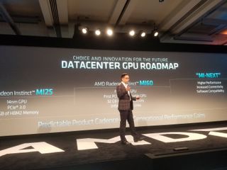
AMD presented its new GPU roadmap. Shipping MI60 this quarter. "MI-Next" is in development, but with no firm date given for delivery.


The 7nm Rome CPUs come with 64 physical Zen 2 cores, which equates to 128 threads per processor, double that of the first-gen Naples chips. In a two socket server, that equates to 128 physical cores and 256 threads in a single box. Rome is also the first PCIe 4.0 CPU, which offers double the bandwidth per channel.
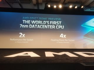
AMD has also made the processors backward compatible with its existing server ecosystem. These drop-in replacements offer twice the performance of the previous generation per socket. You also get four times the floating point performance per chip.

There are eight 7nm eight-core die tied to a central 14nm I/O die.
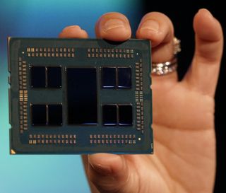
AMD also displayed a demo with the 7nm Rome CPUs and the 7nm GPU MI60 CPUs together. AMD also displayed a single Rome processor beating two of Intel's flagship 8180 CPUs in a rendering benchmark.

Paul Alcorn is the Managing Editor: News and Emerging Tech for Tom's Hardware US. He also writes news and reviews on CPUs, storage, and enterprise hardware.
-
s1mon7 "Zen 2 will provide up to 2X the compute power per node, improved execution pipeline, doubled core density, and use half the energy per operation. AMD has doubled floating point performance with the Zen 2 microarchitecture. "Reply
.....! -
jimmysmitty Reply21463947 said:Feel the hype!
Hype is never good.
21464075 said:"Zen 2 will provide up to 2X the compute power per node, improved execution pipeline, doubled core density, and use half the energy per operation. AMD has doubled floating point performance with the Zen 2 microarchitecture. "
.....!
It seems too good to be true for a die shrink. I can see double the cores doubling performance but halving the energy use while increasing cores? Seems too good to be true. -
s1mon7 Reply21464092 said:It seems too good to be true for a die shrink. I can see double the cores doubling performance but halving the energy use while increasing cores? Seems too good to be true.
"Half the energy per operation" (not per chip). The way I read it is "at the same frequency, now you can fully load twice as many cores as before at the same power ", or "double the number of instructions the core is capable of computing at the same power". The end result is probably a chip with double the cores AND increased processing performance per core to some extent at power per core lower to some extent, where you can in total compute twice as much per Watt, even if the complete chip would use more power than a last-gen chip with half as many cores.
The 14nm->7nm die shrink can do that, with the architecture and IPC improvements filling the gaps of the wider architecture.
Or at least that's what they just claimed, and if their claims are even remotely close to being true, that's probably the most exciting thing in the semiconductor industry since the Core architecture debuted in 2006, if not bigger.
What I also understood to be confirmed, is that we will have 8 cores per CCX. That's prospects of 8-core mainstream chips with no interconnect. That would mean we would have separate dies for <8-core chips from the get-go, and interconnect used only on Threadripper-class chips, and that would be really darn perfect.
-
Giroro Reply21464092 said:
It seems too good to be true for a die shrink. I can see double the cores doubling performance but halving the energy use while increasing cores? Seems too good to be true.
It's halving the energy -per instruction-. That metric wouldn't increase with the number of cores, because an instruction will only execute on one core. So they calculate it using the maths.
Also, the CPU probably has some amount of fixed overhead that will get divided by the number of cores in order to calculate the energy per instruction so I could see at least one way where increasing the number of cores could improve efficiency overall.
So if there's two processors with the same power draw, but one manages to double the number of identical cores within that envelope, then the amount of power per instruction will be halved in the processor with double cores (because it is performing twice as many instructions).
Which is still really good for a process shrink. If I remember correctly, the 28nm to 14nm shrink only improved efficiency by about 30% instead of the 50% AMD is claiming for 14nm to 7nm.
Most Popular

