
ISSCC 2018: The IBM z14 Microprocessor And System Control Design
![]() Archaic to most people, IBM mainframes play a pivotal role in our everyday life. Behind the scenes, these state-of-the-art machines process billions of transactions every day. Announced in July of last year, IBM’s latest mainframe is the z14, succeeding the z13 which launched back in 2015.
Archaic to most people, IBM mainframes play a pivotal role in our everyday life. Behind the scenes, these state-of-the-art machines process billions of transactions every day. Announced in July of last year, IBM’s latest mainframe is the z14, succeeding the z13 which launched back in 2015.
Earlier this year at the 65th International Solid-State Circuits Conference (ISSCC) in San Francisco IBM presented some of the architectural changes between the z13 and z14. The paper was presented by Christopher Berry, a Senior Technical Staff Member for the IBM Systems Hardware Development Team. Mr. Berry led the z14 physical design execution.
z14
For the z14, IBM continued to target the three major vectors that impact customer workloads: increase in per-thread performance, system capacity, and increase efficiency. For the efficiency component, it is important for IBM that the system power footprint remains a constant from one generation to the next in order to facilitate upgrades without requiring costly infrastructure changes. One of the main enablers of those goals is the process technology. As with their POWER9, IBM uses GlobalFoundries’ highly unique 14nm SOI FinFET (14HP) with embedded DRAM in order to extract higher density and reduce the power.
14HP provides them with 17 copper interconnect layers to work with. For the critical metal layer with a 64-nanometer pitch, they use litho-etch-litho-etch (LELE) double patterning technique. This process has two SRAM cells – a high-performance 0.102 μm² cell and a low-leakage 0.143μm² cell. For high-density, they use a 0.0174 μm² embedded DRAM cell which is their workhorse memory cell used for the L2, L3, and the L4 caches.
A Frame
The z14 comes in various models but the max system with processors that can reach 5.2 GHz has to be water cooled. Below is a picture of what a max water-cooled system looks like.
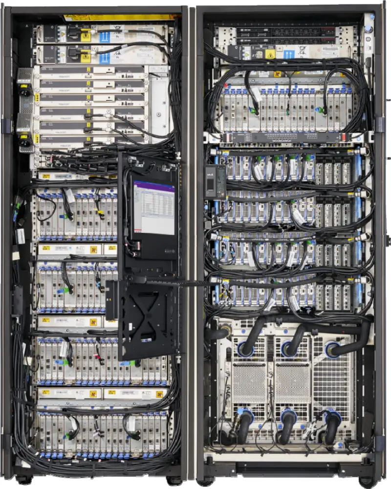
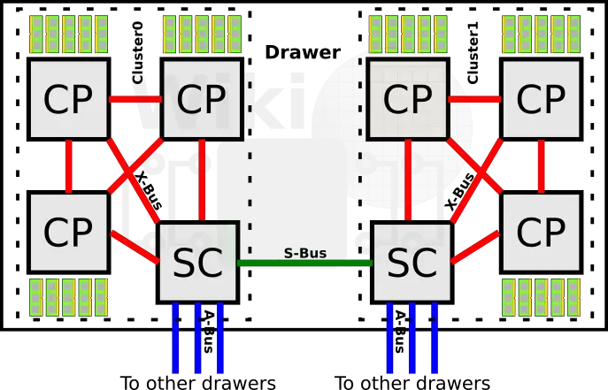
The frames are called A and Z. The more interesting stuff is in the A-frame on the right. The microprocessors reside in the four identically-looking drawers in the middle of the frame.
The Drawer
Each z14 frame features up to four drawers where the CP and SC chips reside. The System Control (SC) chip is responsible for routing the traffic between the four drawers. Every drawer is divided up into two clusters of three processors. Within a cluster, every Central Processor (CP) is fully connected to every other processor as well as to the SC chip. Each CP chip connects to up to 1.5 TiB of main memory and incorporates two PCIe Gen 3.0 interfaces and a GX Infiniband interface.
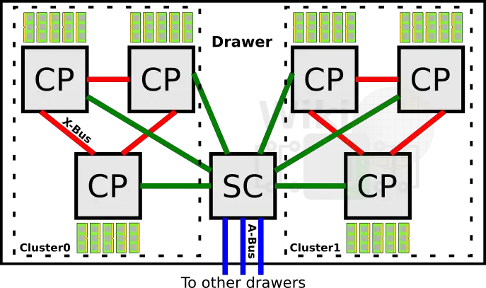
Every drawer is fully interconnected to every other drawer through the SC chips. In a max system configuration, this would produce 24 processors with 240 cores. IBM doesn’t actually sell a 240-core z14 system. The maximum model has 170 cores. 26 additional cores are available for system-assist processors (SAP). SAP cores are designed to assist with the acceleration and offloading of network and I/O processing from the main user-configurable cores. All the remaining cores are left reserved/unusable for power, yield, and sparing purposes. In the z14, each CP chip can support up to 1.5 TiB of main memory with a maximum system support of 32 TiB of memory.
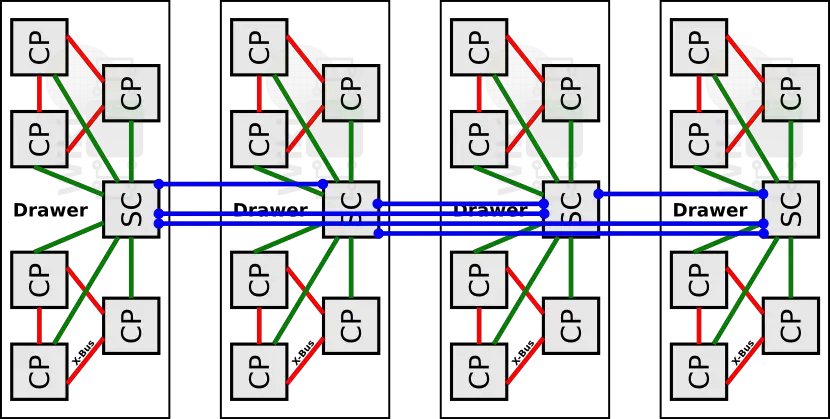
The board wiring diagram below shows the two CP clusters (in orange) and the SC chip (in gray). The two clusters are physically partitioned to the left and to the right of the board with the blue wires fully interconnecting the CP chips within each cluster together. The white and yellow wires connect all the CP chips to the SC chips.
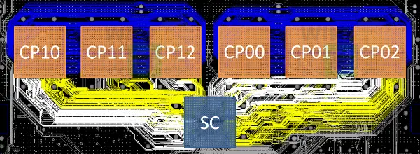
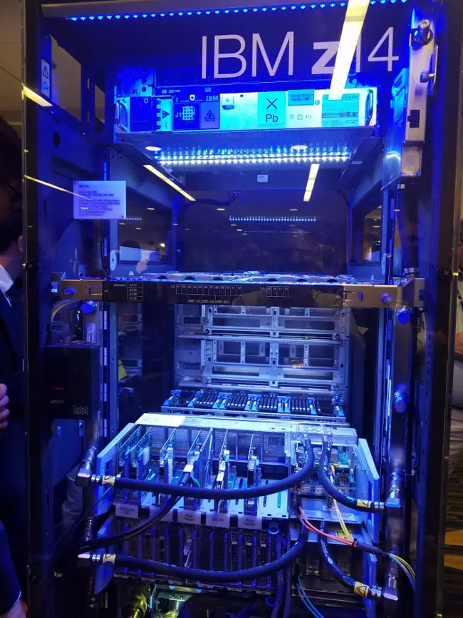
IBM being IBM, a full z14 mainframe was brought to the San Francisco Marriott for the demonstration session. We managed to snap some shots of the drawer for you. One of the water cooling blocks, as well as one of the chips, were specifically sliced to show their cross section.
[foogallery id=”1254″]
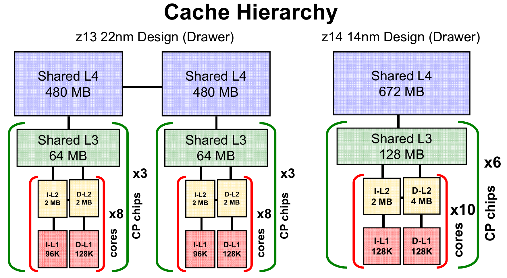
One of the major changes IBM made with the z14 is reorganizing the cache hierarchy of the entire drawer. In their prior machine, the z13, a drawer consisted of two SC chips. Each cluster of three CP chips had their own dedicated SC chip. The two SC chips within the drawer were linked together over the S-bus.
With the z14, the level one instruction cache was increased from 96 KiB to 128 KiB and the L2 data cache was doubled to 4 MiB. The z14 also doubled the shared L3 cache to 128 MiB. The increase in the cache in the lower levels was done in order to be able to remove an entire SC chip from the drawer. The z14 SC chip increased the L4 cache from 480 MiB to 672 MiB, however, since each drawer now has one less SC chip, the L4 cache per drawer was actually reduced by 288 MiB. By removing the second SC chip from the drawer, despite having less L4 cache, due to the latency improvement at the drawer level, the overall change resulted in a performance win.
–
Spotted an error? Help us fix it! Simply select the problematic text and press Ctrl+Enter to notify us.
–