

Often it can be very handy to have a CPU in an FPGA. Though some are sold with an integrated CPU, most are not. A popular option is to use a so called Softcore CPU, a CPU that is implemented in the FPGA’s logic. I decided to have a look at a few popular and some less popular ones to see how easy they are to use, how fast they are and which might be a good choice for a project.
The contenders
I have a few requirements any CPU must meet:
1. There must be a GCC or LLVM compiler available
2. No vendor specific CPU, a CPU should run on all FPGA’s
If possible, a simple ready to go SoC with Uart, Timer and GPIO is nice, but no requirement.
Not that many requirements, so after some googling I found the following options:
- VexRiscv
- LEON3
- PicoRV32
- Neo430
- ZPU
- Microwatt
- S1 Core
- Swerv EH1
Sadly the S1 core and Swerv EH1 did not fit in my Arty board. I tried getting them small enough, but I need the Arty A7-100, so if anyone wants to sponsor me ;)
This still means 6 in total, and there are most likely some other good options as well that I missed.
From looking at the documentation, my gut feeling says that VexRiscv, LEON3 and Neo430 are going to be the nicest to use. I would say that the Microwatt, ZPU and the PicoRV32 are more hobby oriented. But let’s not get ahead of ourselves, each core will be looked at in more detail.
What makes a good Softcore CPU
When using a softcore CPU, I want to be up and running quickly and easily. I also want to be able to add a new peripheral or such if needed.
Speed is a bit of a difficult one. Sometimes a super small CPU that replaces a few state machines is needed, sometimes a more powerful CPU is needed. I decided to look at performance using the still popular Dhrystone benchmark and at the FPGA size so people can pick what they need.
I came up with the following list of things I look for in a Softcore CPU:
Ease of use
- Easy to get up and running
I don’t want to spend evenings to get an example up and running. Changing the pins to match my board and it should be running. - Debugger/bootloader available
Generating everything on each code change is not fun. Ideally a GDB JTAG in the CPU would be great, but some kind of bootloader is also nice. - Good documentation
I think this explains itself - Easy to add a new peripheral
Often when using a CPU in an FPGA, adding a new peripheral is needed. I prefer a known bus like Wishbone or such so it’s easy to connect a new peripheral.
Performance and size
- Performance in DMIPS/Mhz
More speed is more better right :) - Size in LUT/FF
And of course, the smaller the better. - Maximum speed
OK. I lied, more speed is not always better. A CPU that has a maximum frequency of 10Mhz that can do 1DMIPS/Mhz is a lot slower then one that runs at 100Mhz and does 0.5DMIPS/Mhz
Other
- Language used
Mixing Verilog and VHDL is not always fun as not all simulators can deal with it. I don’t have a specific preference, but currently the FOSS tools prefer Verilog, though that is being worked on and likely no issue in the near future. - License
If you want to use a certain CPU in a commercial project, licenses matter.
How to test
I am using my Digilent Arty board to test each CPU. I will use Vivado and either make a Vivado project or, if one is available or can be generated, use that.
To test how easy it is to add a peripheral, I made a small RGB LED peripheral. It has a single 32 bit register, of which 24 bit are used, 8 red, 8 green and 8 blue bits. It generates a PWM signal for Red, Green and Blue based on this. I made this peripheral in SpinalHDL as it’s capable of making a Wishbone, AXI, AHB and other buses peripheral easily.
The code can be found here, a simple test bench is also included.
Vexriscv
Time for the first CPU. I have worked and enjoy working with SpinalHDL so their CPU, Vexriscv, seemed like a good starting point. There are two available SoCs, the Briey and Murax SoC. The Briey SoC a more complex design with SDRAM and even VGA. I went for the Murax SoC as it’s a simpler design.
SpinalHDL generates VHDL or Verilog, and generating a Murax SoC was very easy. I just need to run a single command and as a result an enormous Verilog file is generated. I made a new project in Vivado, added this file and a constraint file that contains the pinning. Press generate bitstream, get some coffee and bam. SoC. It even worked on the first go.
So good points for getting it up and running quickly. Now for debugging: The Murax SoC contains a JTAG debugger that supports GDB. I connected an FT232H module to act as a debugger and then, a problem. OpenOCD with SpinalHDLs patches is needed, which is available as source and not as a precompiled binary. As a result, I need to download and compile OpenOCD and manage another OpenOCD next to my usual OpenOCD. On top of that, it does not even compile on Ubuntu 20.04. Luckily an issue was already opened and contains the fix. After this, this happy screen greeted me.
Customizing the SoC
There is some example code for the Murax here, which compiled with no issues using the prebuild RISCV toolchain from Sifive. To add my own peripheral, I made a new project based on the Murax example, but with some of the parts I do not use removed. I don’t need to generate for 5 different targets, just the one for me :)
Adding the RGB peripheral was not too bad, just different from working in Verilog or VHDL. This is one of the downsides compared to other CPUs, to work with it it can be helpful to learn some SpinalHDL. A bit of fidgeting later and I had a working blink a RGB LED.
Vexriscv itself is very configurable, from a small CPU like used in the Murax to a Linux capable CPU, neat.
Performance
Can’t test a core without some benchmarks. Murax can be build as default or fast core, but as it’s aimed to be a small core, performance is not earth shattering. Vexriscv is capable of 1.57DMIPS/Mhz, but the Murax SoC promises 0.45 or 0.65DMIPS/Mhz depending on build configuration. I got 0.52 and 0.75DMIPS.Mhz. For context, an ARM M0 achieves around 1DMIPS/Mhz
In terms of size, in fast configuration the entire SoC uses 1206 LUTs and 1373 Flipflops, in other words, about 5% of the FPGA. The CPU by itself uses just 769LUTs and 665FF’s
When I build it for size, the entire SoC is 1074LUTs and 1338FF’s and the CPU is just 648LUTs and 630FF’s. In terms of speed, for the entire SoC the maximum speed is 146/127Mhz for default and fast setting.
Conclusion
All in all I quite like the Vexriscv CPU and Murax SoC. They can be customized into a small CPU or a CPU with pretty great performance. I do think a few things still can be improved. Firstly, having to compile OpenOCD can be a hassle, providing prebuild binaries would be nice. Secondly, the peripherals for the SoC are not very well documented.
I personally like SpinalHDL, but I can understand not everyone wants to learn a new language when trying out a CPU. Luckily pre-generated cores also can be found here.
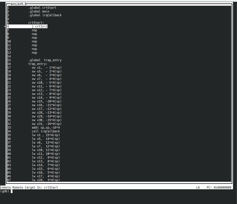
LEON3
I’ll jump right into the next one, LEON3. LEON3 is a SPARC V8 compatible CPU written in VHDL. LEON3 is a mature CPU, it has been used in ASICs and even in space, neat. It is bundled with a lot of extra libraries to make a SoC, so let’s give it a try.
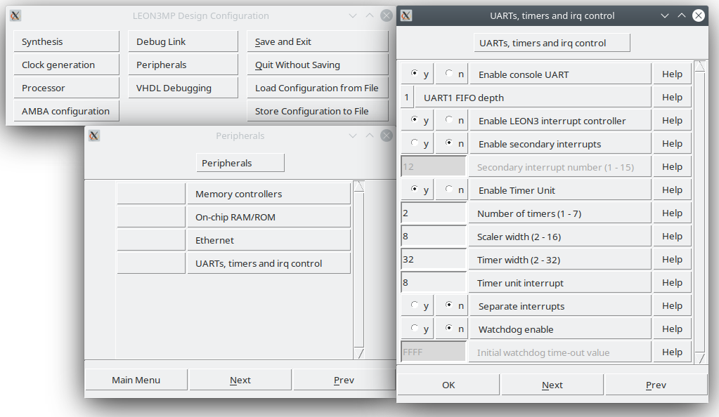
Included in the download are a lot of example projects for different development boards, some example software and a lot of documentation. For example, the included peripherals are well documented, and the same goes for the CPU. I am quite happy to see this as this is not always the case. I also like the tool used to configure the SoC. After executing make xconfig you are greeted with a GUI to adjust the SoC.
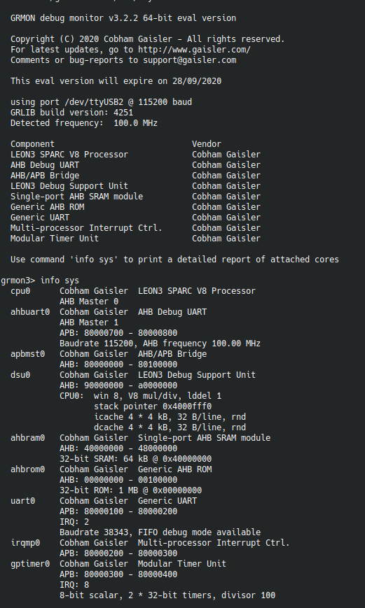
The example for my arty board was up and running quickly. This gave me a change to look at the debugger. The debugger is not the usual JTAG and GDB combo, but a custom debugger called GRMON. GRMON can use different interfaces, in my case I used a serial port to connect to the CPU. GRMON works quite nicely, giving a very usable command line interface to interact with the SoC. The evaluation version of GRMON does lack some features like a GUI, but it’s good enough to try the CPU out. It even reads the SoC info and shows this in the command line.
Compiling my own code did not work as quickly. The compiler suite can be downloaded online, but compiling some code gave me incorrect binaries. Also nice, the makefile to build the software did not seem to work. After some trial and error I found this great repository containing working makefiles and a dhrystone program, nice.
Customizing the LEON3
I already touched on customizing the SoC, which works via a nice GUI tool. But I want to be able to add my own peripheral as well. LEON3 uses the APB3 bus, luckily I made my PWM peripheral in SpinalHDL which also supports this bus. After a quick change and generate later I had a APB3 version of my peripheral. However, getting it to work did not go as smooth as I wanted.
The nice information screen the GRMON tool reads out has to come from somewhere, and indeed, every peripheral has a vendor and type, and without one it seems to not work. I added a none existing Vendor/type but the evaluation version of GRMON only supports certain vendors/type. I gave the PWM peripheral the same vendor/type as the included timer peripheral and that worked, although the information screen is a bit less useful like that.
Performance
The other important thing, performance. I got 0.84DMIPS/Mhz, which is less then the promised 1.4DMIPS/Mhz. I played around a bit with the configuration but could not get more, perhaps a compiler setting or such that is incorrect. Sadly there is no exact info on how the 1.4DMIPS/Mhz is achieved, so that makes it hard to reproduce. The maximum clock speed on my arty is around 85Mhz for this CPU.
LEON3 is a bit of a big SoC, clocking in at 5505LUTs and 2224FF’s. The CPU takes up the biggest part at 4542 LUTs and 1552FFs.
Conclusion
LEON3 is not the smallest nor fastest SoC, but it is well supported. The documentation is very good and being able to get commercial support can be very handy. The example code might be something that could be improved though.
I do like the LEON3 SoC. It might not be the best hobby SoC and it’s fairly big, but for professional work it looks like a great choice.
PicoRV32
Another RISC-V CPU, a popular one at that. PicoRV32 is a RISC-V CPU aimed at high clock speeds and a small size. Therefore, performance is relatively slow. PicoRV32 is a single verilog file and includes a wishbone and axi version of the CPU as well
An example SoC exist, meant for an ICE40 FPGA exist called the picosoc. This uses the flash memory on the ICE40 dev board and seemed a hassle to port. I instead decided to make my own SoC, how hard can it be :)
I created a SpinalHDL wrapper around the wishbone variant of the PicoRV32 and added a few peripherals, including my RGB peripheral of course. As I made several small wishbone peripherals before in Spinal, I had a working SoC in about 2 evenings.
I had no debugger or boot loader, but this is similar to the picosoc. Compiling code turned out a bit more annoying then I had hoped for. I already have the RISCV toolchain installed from the Vexriscv. However, the example makefiles use a different version of the toolchain. There is a script included that downloads and compiles the toolchain, but yet another toolchain is a bit annoying. Apart from that, making a SoC went fairly smooth thanks to the wishbone interface and SpinalHDL.
Customizing the PicoRV32
As I made the SoC, I cannot look into customization of the SoC. However, I can look at customizing the PicoRV32 CPU. The PicoRV32 core can be configured as a very small CPU. It can even be used with just 16 registers (RISC-V e core) With all options on, it supports the multiplication and compressed RISC-V ISA. Supporting a simple memory interface as well as wishbone and AXI also aids in customizability.
Performance
As I mentioned in the PicoRV32 intro, it is not meant as a very fast CPU. On the github a speed of 0.305DMIPS/MHz is mentioned when not looking the look-ahead memory interface. If that interface is used, the speed is 0.516DMIPS/Mhz. In practice using my SoC I got 0.2DMIPS/Mhz. This is most likely due to the wishbone interface being a bottleneck. I also tried with the multiply and compressed instruction support disabled and got 0.188DMIPS/Mhz.
Clock speed is more impressive however. I got 170Mhz for my SoC with multiply and compressed disabled. With those enabled I got around 130Mhz.
Looking at size, multiply/compressed disabled my entire SoC is 1134 LUTs and 889FFs. The CPU takes 1000 LUTs and 701FFs. With multiply and compressed ISA enabled the CPU needs 2011 LUTs and 1213 FFs.
Conclusion
PicoRV32 is a popular hobby CPU, with some good reasons. It is quite configurable in CPU size and supports multiple busses. However, in terms of software some steps can be made. There not being a ready to use SoC for various boards is also a bit of a bummer.
When looking at another popular RISC-V CPU, the Vexriscv, I do not see a lot of reasons to use PicoRV32. Vexriscv is small, comes with 2 different SoCs and has a GDB debugger.
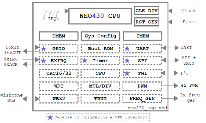
NEO430
After all the 32 bit CPUs, time for a 16 bit one. The NEO430 is a CPU compatible with the TI MSP430 series. The MSP430 promises to be a small, microcontroller like SoC, so let’s have a look.
The NEO430 is more of a microcontroller then a CPU as it comes with a lot of peripherals. For instance, when fully configured, it includes I2C, SPI, Timers and more.
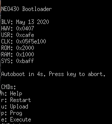
Using the NEO430 was a nice experience. There are no example project, but adding all VHDL files and setting the pins correct is all that I needed to do. Peripherals are enabled or disabled via a couple of generics in the top level, making customizing easy. The NEO430 lacks a debugger, but by default it has quite a handy bootloader. It even has a nice menu:
Getting code to compile and run went with no big issues either. The toolchain can be downloaded from TI as it’s an MSP430 compatible CPU. There also are a lot of example software projects to start with. I also quite like the documentation, which is over 90 pages of nice document, even including a good getting started section.
Customizing the MSP430
After all the praise, I finally ran into an issue when adding my PWM peripheral. The MSP430 supports the wishbone bus, however, in the documentation this is mentioned:

My wishbone peripheral did not like this at all. I had to change it around a bit to get it up and running. Another thing that is a little bit of a bummer is that the peripherals are fixed. I can disable or enable UART, but not easily add a second UART.
Performance
It’s a bit slow. With multiply/divide enabled I got 0.154DMIPS/Mhz. The NEO430 doesn’t claim to be fast, it claims to be small. And small it is. With just 863 LUTs and 821 FFs for the entire SoC. The CPU is just 420 LUTs and 126 FFs, nice.
In terms of clock speed the SoC can run at 100Mhz on my arty board.
Conclusion
I quite like this small CPU. There is a lot to like. Getting it up and running went smooth, the documentation is pretty great and it’s really small. The NEO430 is not the fastest CPU on the block, but when you do not need a number cruncher of a CPU, it’s great. However, there is a small potential issue.
The NEO430 uses the MSP430 instruction set, which is not a free and open source instruction set like RISC-V or SPARC. On the other hand, MSP430 is quite old so patents might have run out. For hobby use it’s probably fine, but for commercial use a quick talk with a legal advisor might be handy.
ZPU
Ah, the ZPU. I used the ZPU cpu before, it was one of the reasons I got my first fpga board, one of the Papilio boards so I could play with the zpuino. The ZPU is a 32 bit stack based CPU. It was made to be the smallest CPU that GCC could target. The ZPU is a stack CPU, meaning it does not have registers like most CPUs do. The ZPU also has a very small number of instructions that are mandatory. A lot of the instruction set can be emulated in software using the small set of mandatory instructions. All this to make it small.
As I used the Zpuino before, I gave it a go. Sadly, getting it to run in Vivado did not work out. The git repo is a bit unorganized and there are only example projects for older spartan fpga’s. Luckily ZPU is an open architecture and someone made the ZPUFlex. There are even a couple of peripherals and demo projects, very nice.
ZPUFlex was up and running quickly. There is no debugger or bootloader, but it synthesizes very quickly luckily. Getting hello world to run went fast and with no big issues.
Compiling code went reasonable. GCC can be downloaded as binary. However, ZPU is the smallest CPU with GCC support, but the version is, well. Ancient. GCC 3.4.2 is the latest, and there is no newer version being made by the looks of it.
Customizing the ZPUFlex
The ZPUFlex does not support wishbone or some other bus in order to be very small. A simple memory bus is supported, and connecting a peripheral is fairly straightforward.
The ZPUFlex has a good amount of configuration options. For example to enable or disable parts like the multiplier, emulated instructions and more.
Size
Yes, I called it size and not performance as, honestly, there is not much performance :)
The ZPU is tiny. really tiny. A small SoC with a uart is 469 LUTs and 287 FFs The CPU alone uses 369 LUTs and 189 FFs.
Performance is, well. slow. In a small configuration it does 0.014DMIPS/Mhz. At 50Mhz it’s as fast as the Vexriscv at 1Mhz. With some options like multiply and such on it does 0.06DMIPS/Mhz. This matches the claims in the dhrystone example at least.
In clock speed, it’s the fastest at around 215Mhz, so that’s something. A simple CPU generally means a high clock speed and the ZPUFlex matches that.
Conclusion
The ZPUFlex core was up and running quickly and performs about as I expected. Slow, but very small. The ZPU architecture is an odd and interesting one. Sadly development of the toolchain is kind of non existing, but it’s definitely an interesting CPU architecture wise. For a small CPU, the NEO430 is most likely a better choice
Microwatt
A while ago, IBM decided to make their POWER architecture open source. This means everyone can make and use a POWER CPU, which is always good news. Microwatt is a POWER ISA CPU written in VHDL that was launched almost simultaneously.
Microwatt uses FuseSoC in order to support several FPGA boards, including the Arty board I got. This makes it easy to generate a Vivado project and try it out. Recently support for ECP5 Lattice FPGA’s is also being worked on, so some more boards probably will be supported soon.
The SoC includes DDR3 memory support and UART. When I tried it out there was no debugger or bootloader, but it seems work is being done in getting that running as well. No timer is included currently, so for running some benchmarks, I added a simple timer.
Software wise, the hello world example compiled without any issues. There is also micropython support, which is kinda neat. There are not a lot of examples, but there are also not a lot of peripherals to write examples for.
Customizing the Microwatt
I started by adding a simple timer. Microwatt uses the wishbone bus, so adding a timer went pretty easily. As synthesizing the Microwatt CPU takes a while and the lack of debugger/bootloader means a synthesize for each code change, I did not add the PWM peripheral.
Microwatt has a few configuration options, but cannot be customized in the way some other CPUs can.
Performance
Let’s see what this POWER CPU can do. A quick Dhrystone benchmark gave me around 0.5DMIPS/Mhz. Not the fastest CPU, but not too bad. There is no claimed speed anywhere on their github, so I cannot verify if my result is correct or not.
POWER is a 64 bit CPU, making it not a very small CPU. Microwatt needs 7337 LUTs and 3465 FFs in the Arty FPGA. It can run at a little over 100Mhz.
Conclusion
I think it’s really cool that an open source POWER CPU exists. Microwatt is still in active development and in the month or so between trying it and writing the blog post quite some stuff has been added. Documentation is sadly not a strong point at the moment, hopefully this will improve in the future.
Looking at size and performance, Microwatt is not the fastest nor smallest CPU. If I need a CPU in an FPGA, it would not be my first choice. However, more choice in CPU’s and CPU architectures is always welcome.
Swerv EH1
Sadly, the Swerv EH-1 core did not fit in my fpga. I need about twice the FPGA for that to work. I do want to write a bit about the Swerv EH-1 core as it’s an interesting beast.
Western Digital, the famous hard drive company, made the EH-1 core as a high performance CPU for embedded use. They recently also added the EL-2, a smaller core that is a bit slower and the EH-2, a dual threaded higher speed EH-1 variant. The claimed performance of the EH-1 CPU is 2.9 DMIPS/Mhz, which is pretty amazing. Tom Verbeure has a great blog post about this design.
What I find the most interesting is that a big company is making their RISC-V cores open source, something that is rarely done.
OpenSPARC S1
Of course, rarely is not never. Sun has released some of their server CPU’s back in 2005. The Ultrasparc T1 and T2 designs are open and can be found online.
The T1 in an 8 core, 32 thread Sparc V9 core, the T2 can do 8 threads per core, making it an 8 core 64 thread CPU. These CPUs where pretty fast when released. Of course, putting an 8 core server CPU in an FPGA won’t fit at all.
There is a single core, 1 to 4 thread version, called the S1 core. Sadly, even this design does not fit in my Arty board. Depending on synthesizing it with 1 or 4 threads, it needs between 40 to 60.000 LUTs
Performance wise, it probably is no match for something like the Swerv cores, but it is an interesting historical CPU and one of the few times a commercial CPU design has been made open source.
Comparison and conclusion
6 softcores later, it’s time to make up the balance.
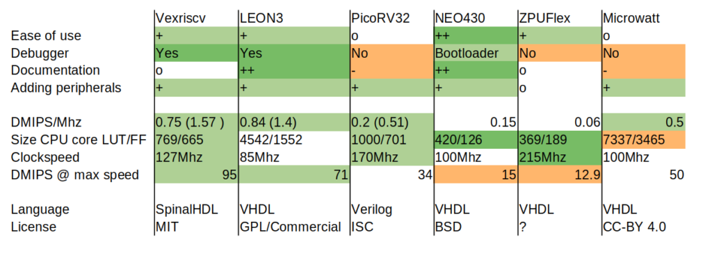
If I got a different DMIPS/Mhz result then claimed, I added the claimed result in brackets as well. Ratings can be -, o, + or ++, and are very much just my opinion.
I liked the Vexriscv, LEON3 and NEO430 the most in terms of usability. None of them where perfect. Vexriscv is very flexible, but lacks documentation in some areas, LEON3 probably works perfect with a commercial license and the NEO430 lacks a debugger. But all in all, those three seem the best choices in my opinion if you need a CPU for an FPGA project.
Some things stand out. 4 cores are 1000 LUTs or smaller and the other 2 are a lot bigger. This most likely is due to build in multiplier/divider blocks, which can be disabled on a CPU like Vexriscv. With 6 CPU’s tested I have tried 5 different CPU architectures. Only RISCV was in 2 CPU’s, but there are a lot of other RISC-V CPU projects.
All in all, this was a fun project to do, and took quite some evenings in total. There are a lot of other CPU’s and I cannot test them all. And frankly, I have seen enough CPU’s for now :)
All the code, Vivado projects and such can be found on my github. If you enjoyed this pretty long post, you can buy me a coffee.
Nice to see ZPUFlex – one of my previous pet projects – getting a mention there! I realise you’ve had enough of CPUs for now, but others that are well worth a look are TG68K (MC68000/020 compatible, respectable though not superb speed, a bit porky, but M68K’s still a nice architecture), f32c (MIPS/RISC-V configurable, pretty modest size in MIPS configuration, and *very* fast – 1.63 DMIPS/MHz), and my newest project, EightThirtyTwo (32-bit CPU with eight bit instruction words. A bit bigger than ZPUFlex, but also a fair bit faster – but the main aim was good code density and minimum possible use of block RAM. No GCC/LLVM, but a backend for the vbcc C compiler, and also a JTAG debugger, though currently Altera/Intel only.) I have demo SoCs for all three in the same github as ZPUFlex.
Thanks for your comment.
I have tried f32c a while ago, but completely forgot about it when making this blog post. I had no idea it could be configured to run that fast, pretty neat.
I agree the 68K is a nice architecture, I got an 030 chip here to sometime make a nice machine, perhaps a future blog :)
The EightThirtyTwo looks nice too, I understand you created the vbcc backend yourself? I can imagine that costing a good bit of time, I might try it out in the future.
Rik
Yes, the vbcc backend took a fair bit of time, but I believe it took an order of magnitude less effort than understanding and then implementing something similar for GCC or LLVM – and isn’t such a fast-moving target, so less likely to suffer bit rot. VBCC’s backend interface is (a) well designed, and (b) well documented, with a “generic risc” backend as a kind of template for new architectures, too. The only downside of vbcc is an unusual license, with permission required for commercial usage. The author’s very approachable and supportive, though.
I look forward, one day, to reading about your ‘030’s future adventures!
Interesting read. I would suggest looking at least at the following additions;
– mor1kx (https://github.com/openrisc/mor1kx)
– J-Core (https://j-core.org/)
– LatticeMico32 (https://github.com/m-labs/lm32)
There are also a ton of other RISC-V CPUs you could try out too!
– minerva (https://github.com/lambdaconcept/minerva)
– Taiga (https://gitlab.com/sfu-rcl/Taiga)
– Rocket — For RISC-V 64bit (https://github.com/chipsalliance/rocket-chip.git)
– serv — Probably the **smallest** RISC-V 32bit core here (https://github.com/olofk/serv)
– CV32E40P — https://github.com/antmicro/cv32e40p
The LiteX environment supports most of these and you can switch between them without changing the rest of your design! See @ https://github.com/enjoy-digital/litex/wiki/Soft-CPU
Lastly, that VexRISCV Fmax seems a little low? See the Area / Frequency reports that they publish at https://github.com/SpinalHDL/VexRiscv#area-usage-and-maximal-frequency (and these are a bit out of date, things should be smaller and faster now).
If you want to go crazy, you can also look at multiple soft cores! https://antmicro.com/blog/2020/05/multicore-vex-in-litex/
microwatt, mor1k, j-core, vexriscv and rocket all also support running Linux on your softcore. That could be another interesting direction to explore!
There are a ton of great softCPUs to look at, more then I have time to try out sadly enough :)
I have played around with the multicore SoC, having 4 CPU’s in my FPGA board was very satisfying to see run.
Regarding the Fmax, they synthesized using the fastest speed grade, while my Arty board has the 1L (slower and low power) speed grade. This could explain the difference in Fmax between my results and their page.
4 RISC-V CPUs in an FPGA is pretty cool but if you go with SERV you can have 5807 RISC-V cores instead ;)
https://twitter.com/OlofKindgren/status/1265170129911980032?s=19
(You can’t do very much with each core in this configuration though, but still)
Haha, small difference in the kind of CPU yeah. But Serv is really quite neat and insanely small :D
Totally understand!
I wouldn’t expect to see such a big difference between the 1L and faster speed grade. What timing constraints are you giving to Vivado? Vivado might just be stopping because it is “good enough”?
Selecting the fastest speed grade of the same FPGA gives me an FMax of 238Mhz, so it seems that just the faster speed grade makes a ton of difference.
That is super interesting!
Do you want to post a github issue on the VexRISCV asking them (us) to provide CPU benchmark for the different speed grades? You might find that in the process fmax goes up :-)
You should also consider using embench for your benchmarking. Using CoreMark or Drystone makes David Patterson cry –> https://www.sigarch.org/embench-recruiting-for-the-long-overdue-and-deserved-demise-of-dhrystone-as-a-benchmark-for-embedded-computing/
I used Dhrystone as it’s one I am familiar with, I have used coremark before but embench is new for me. I’ll have a look at it for future projects, thanks for the link.
Interesting article! Just for reference the Cortex-M3 can be synthesized for any FPGA. The licensing is a bit shit as it’s only good for commercial use on Xilinx and Gowin tho. ARM has released two different implementations, one is an obsfucated/flattened plaintext core that can be used anywhere, the other has an encrypted p1735 wrapper so it can only be used with Vivado.
I built a wrapper using Olof’s most excellent fusesoc with a simple blinky project. https://github.com/tinylabs/tinylabs-cores. Fmax on the Arty is ~30MHz for the obsfucated and ~50MHz for the encrypted.
Oh cool, I knew ARM was being a bit more lenient with their cores lately, but I thought the M3 only was for Vivado. Probably remembered it incorrectly.
Thanks for the info :)
They only market it for Vivado through there designstart FPGA program. The Gowin development is pretty recent. The flattened version is buried in their designstart Eval package (AT421). Haven’t seen anyone else use it but given it’s just verilog it should synthesize on any FPGA fine.
Great Job!
I’ve been looking for a soft cpu, targeting FPGA, for a while.
RISC-V is a clear election to me, but there are a bunch of cores available and it’s not easy to select one of them.
Vexrisc: in spinalHDL, another HDL languaje, not please!.
PicoRV32: Not easy to use, not documentacion, not debugger.
I’m not sure which one to choose.
Hello,
what changes should be made in the constraints file for arty a7-100 FPGA for the murax verilog to run?
I personally like SpinalHDL too, but it’s the last language I will learn. I’m getting too old now! lol
Great post, I learned a new way to look at things!