This is a guest post. The views expressed here are solely those of the authors and do not represent positions of IEEE Spectrum or the IEEE.
Light detection and ranging, or lidar, is a sensing technology based on laser light. It's similar to radar, but can have a higher resolution, since the wavelength of light is about 100,000 times smaller than radio wavelengths. For robots, this is very important: Since radar cannot accurately image small features, a robot equipped with only a radar module would have a hard time grasping a complex object. At the moment, primary applications of lidar are autonomous vehicles and robotics, but also include terrain and ocean mapping and UAVs. Lidar systems are integral to almost all autonomous vehicles and many other robots that operate autonomously in commercial or industrial environments.
Lidar systems measure how far away each pixel in a 3D space is from the emitting device, as well as the direction to that pixel, which allows for the creation of a full 3D model of the world around the sensor. The basic method of operation of a lidar system is to transmit a beam of light, and then measure the returning signal when the light reflects off of an object. The time that the reflected signal takes to come back to the lidar module provides a direct measurement of the distance to the object. Additional information about the object, like its velocity or material composition, can also be determined by measuring certain properties of the reflected signal, such as the induced Doppler shift. Finally, by steering this transmitted light, many different points of an environment can be measured to create a full 3D model.
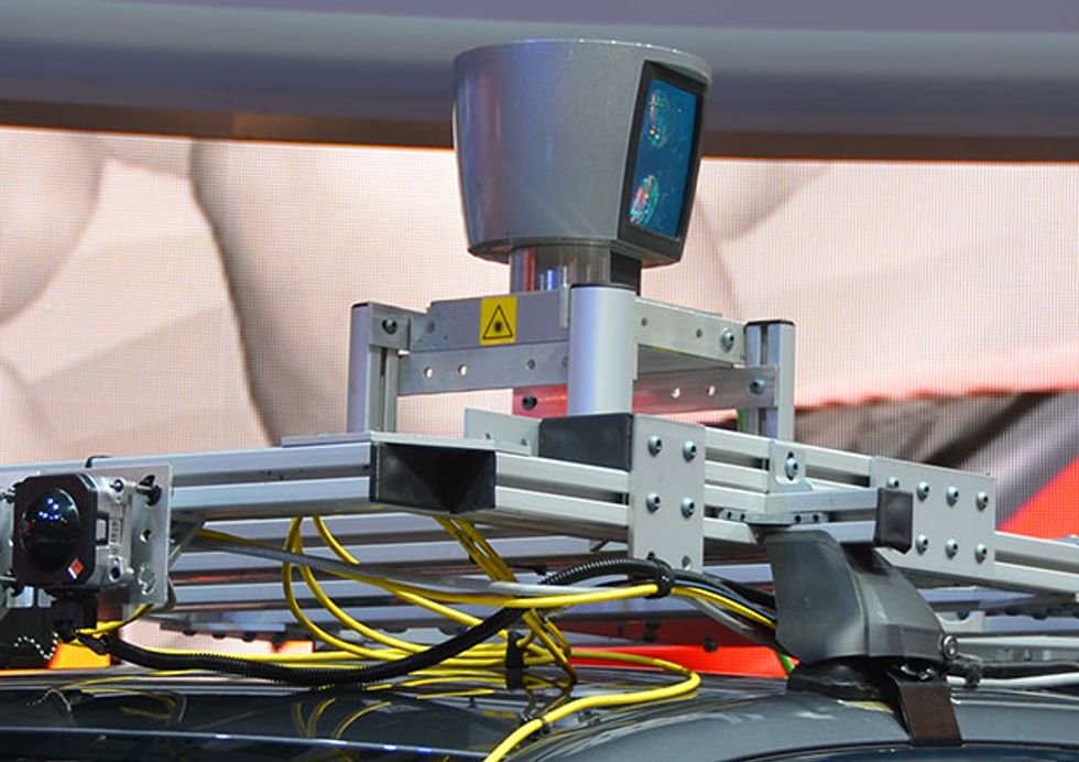 Velodyne HDL-64 lidar mounted on a self-driving car. The device uses a laser/receiver module that is mechanically spun around, an approach that limits the scan rate of the system while increasing size, complexity, and cost.Photo: Evan Ackerman/IEEE Spectrum
Most lidar systems—like the ones commonly seen on autonomous vehicles—use discrete free-space optical components like lasers, lenses, and external receivers. In order to have a useful field of view, this laser/receiver module is mechanically spun around, often while being oscillated up and down. This mechanical apparatus limits the scan rate of the lidar system while increasing both size and complexity, leading to concerns about long-term reliability, especially in harsh environments. Today, commercially available high-end lidar systems can range from $1,000 to upwards of $70,000, which can limit their applications where cost must be minimized.
Applications such as autonomous vehicles and robotics heavily depend on lidar, and an expensive lidar module is a major obstacle to their use in commercial products. Our work at MIT's Photonic Microsystems Group is trying to take these large, expensive, mechanical lidar systems and integrate them on a microchip that can be mass produced in commercial CMOS foundries.
Our lidar chips are produced on 300-millimeter wafers, making their potential production cost on the order of $10 each at production volumes of millions of units per year. These on-chip devices promise to be orders of magnitude smaller, lighter, and cheaper than lidar systems available on the market today. They also have the potential to be much more robust because of the lack of moving parts. The non-mechanical beam steering in this device is 1,000 times faster than what is currently achieved in mechanical lidar systems, and potentially allows for an even faster image scan rate. This can be useful for accurately tracking small high-speed objects that are only in the lidar's field of view for a short amount of time, which could be important for obstacle avoidance for high-speed UAVs.
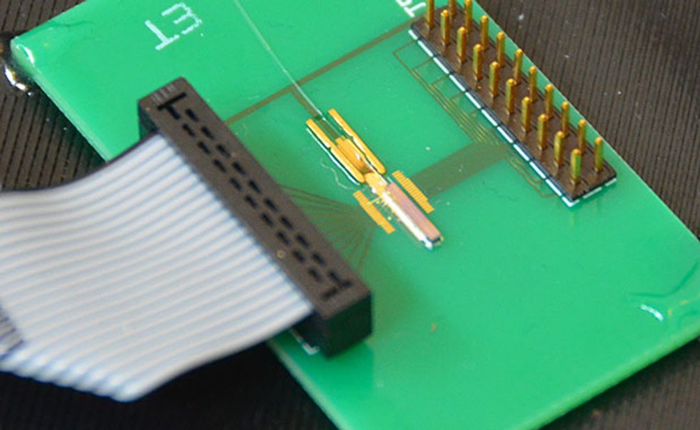 MIT's prototype lidar chip operating at DARPA's Pentagon Demo Day in May 2016.Photo: Evan Ackerman/IEEE Spectrum
At MIT our lidar on a chip work first began with the development of 300-mm silicon photonics. Silicon photonics is a chip technology that uses silicon waveguides a few hundred nanometers in cross section to create “wires for light," with properties similar to optical fibers except on a much smaller scale. These waveguides are then integrated into on-chip photonic circuits. An electronic analogy to silicon photonics would be something like taking discrete electrical components, such as copper wires and resistors, and integrating them onto a microchip with copper traces and nano-scale transistors.
Microelectronics, particularly CMOS technology, has allowed for much smaller and complex electronic circuits that can be mass-produced, and silicon photonics has the potential to do the same for photonics as microelectronics has done for the electronics industry. Silicon photonics can leverage the technology of commercial CMOS foundries, the same technology that develops the silicon-based microprocessors in computers, in order to be mass-produced at a very low cost. Over the past decade, several CMOS foundries have developed dedicated silicon photonics fabrication processes. Through this development process, fundamental issues such as waveguide loss and optical isolation were addressed and the technology is now at a state where complex photonic systems can be created.
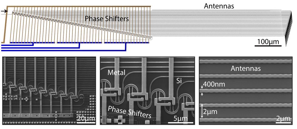 A scanning electron microscope image of MIT's solid-state lidar. The device uses thermal phase shifters to heat the waveguides through which the laser propagates, changing the speed and phase of the light that passes through them. Notches fabricated in the silicon act as antennas, scattering the light into free space, and constructive interference is used to focus the beam without a need for lenses.Image: Christopher V. Poulton
The Defense Advanced Research Projects Agency (DARPA) is interested in the scalability and integration of silicon photonics with electronics, and created the Electronic-Photonic Heterogeneous Integration (E-PHI) program in 2011. Two major accomplishments of this program were the first large-scale optical phased array and the first array with a wide-angle steerable beam. These devices demonstrated that practical optical phased arrays could be fabricated in commercial CMOS foundries, much like electronic phased arrays have been for decades. Electronic phased arrays have been used in radar applications for non-mechanical radio beam steering, and optical phased arrays seemed like a very elegant solution for a small, low-cost, solid-state lidar.
Our device is a 0.5 mm x 6 mm silicon photonic chip with steerable transmitting and receiving phased arrays and on-chip germanium photodetectors. The laser itself is not part of these particular chips, but our group and others have demonstrated on-chip lasers that can be integrated in the future. In order to steer the laser beam to detect objects across the LIDAR's entire field of view, the phase of each antenna must be controlled. In this device iteration, thermal phase shifters directly heat the waveguides through which the laser propagates. The index of refraction of silicon depends on its temperature, which changes the speed and phase of the light that passes through it. As the laser passes through the waveguide, it encounters a notch fabricated in the silicon, which acts as an antenna, scattering the light out of the waveguide and into free space. Each antenna has its own emission pattern, and where all of the emission patterns constructively interfere, a focused beam is created without a need for lenses.
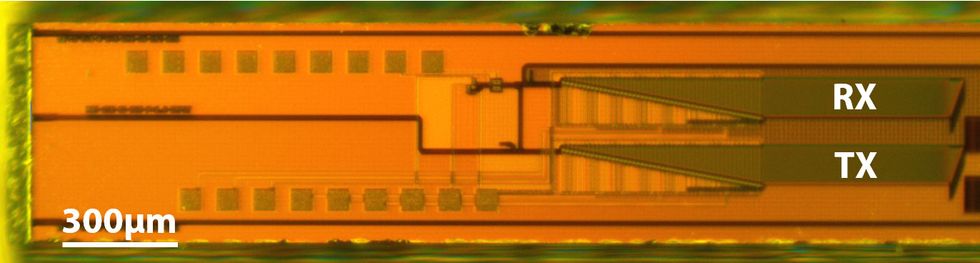 Optical micrograph shows MIT's solid-state lidar, a 0.5 mm x 6 mm silicon photonic chip with steerable transmitting and receiving phased arrays and on-chip germanium photodetectors.Image: Christopher V. Poulton
The current steering range of the beam is about 51°, limited by the spacing between the antennas. Reducing this spacing becomes challenging because there is a limitation to how small silicon waveguides can be while still confining light adequately, although our technology should support near 100° steering. Even with a limited steering range, one could imagine placing multiple lidar sensors on a vehicle in order to get a full 360° image.
The detection method in our lidar is based on a coherent method instead of direct time-of-flight measurement, where the system only reacts to the light that was originally transmitted by the device. This reduces the effect of sunlight that can be a large noise factor in lidar systems, and allows for modest photodetectors instead of expensive avalanche photodetectors or photo-multiplier tubes that are challenging and expensive to integrate in a silicon photonics platform.
At the moment, our on-chip lidar system can detect objects at ranges of up to 2 meters, though we hope to achieve a 10-meter range within a year. The minimum range is around 5 centimeters. We have demonstrated centimeter longitudinal resolution and expect 3-cm lateral resolution at 2 meters. There is a clear development path towards lidar on a chip technology that can reach 100 meters, with the possibility of going even farther.
Using other materials in the chip (such as silicon nitride) will allow for an increase in power output of two to three orders of magnitude. Our fabrication process includes silicon nitride layers along with silicon that allows for systems utilizing both. Additionally, a larger phased array would allow for less diffraction (spreading out) of the beam, resulting in longer ranging and higher lateral resolution. The challenge here is how uniform and precise the silicon waveguides and antennas can be fabricated, and this capability will most likely increase in the future as lithography technologies improve. Though we have had promising results in creating very-large scale phased arrays for lidar applications, the question of how large they can be reliably fabricated is still unknown, and will most likely be the limiting factor of the range of this technology in the future.
DARPA has recently created a follow-up program called Modular Optical Aperture Building Blocks (MOABB), which is focused on extending this silicon photonic lidar work in the coming years. Though the MOABB program is not a part of our academic research group, after the lidar effort of the E-PHI program ends, we plan to extend our phased array work to free-space communications to allow for multiple photonic chips to interface with each other with >40Gb/s data rates. We are also developing visible light phased arrays with applications such as Li-Fi and holography that can be seen by the human eye.
We believe that commercial lidar-on-a-chip solutions will be available in a few years. A low-cost, low-profile lidar system such as this has many applications in autonomous vehicles and robotics. It would allow for multiple inexpensive lidar modules to be placed around a car or robot. These on-chip lidar systems could even be placed in the fingers of a robot to see what it is grasping because of their high resolution, small form factor, and low cost. These developments have the potential to dramatically alter the landscape of lidar systems by changing how the devices operate and opening up the technology to numerous new applications, some of which have not even been thought of today.