Original Link: https://www.anandtech.com/show/10347/arm-cortex-a73-artemis-unveiled
The ARM Cortex A73 - Artemis Unveiled
by Andrei Frumusanu on May 29, 2016 11:00 PM EST- Posted in
- Arm
- Mobile
- ARMv8
- Artemis
- Cortex A73
It’s only been a little over a year since we had a good look into ARM’s Cortex A72 presented at ARM’s TechDay event in London. Over the span of this year we’ve seen various vendors not only announce SoCs with the new core IP but actually deliver devices in high volume. HiSilicon’s Kirin 950/955 definitely left a long-standing impression on the industry by providing incredible power efficiency gains while continuing to improve performance.
Fast-forward to 2016. Another year, another TechDay, this time from ARM’s brand-new offices in Austin Texas. So for today we have the pleasure to have a very deep look at ARM’s new Artemis CPU microarchitecture:
A Look Back At Recent History
The Cortex A73 is ARM’s new premium mobile CPU micro-architecture meant to succeed the Cortex A72 in consumer segments. Before we dive into details of the new CPU, it’s important to try understand and recap ARM’s CPU recent microarchitectures released the last few years.
The Cortex A9 was an incredibly important design for ARM as, in my view, it provided the corner-stone for SoC and device vendors to create some of the designs that powered some of the most successful devices that brought with them a turning-point in smartphone performance and experience. Apple’s A5, Samsung’s Exynos 4210/4412, and TI OMAP4430/4460 were all SoCs which made the A9 a very successful CPU micro-architecture.
Following the Cortex A9 we saw the introduction of the Cortex A15. The core was a substantial jump in terms of performance as it provided the single largest IPC improvement in ARM’s Cortex A-profile of application processors. While the A15 represented a large performance boost, it came at significant cost in terms of power efficiency and overall power usage. It took some time for the Cortex A15 to establish itself in the mobile space as the first designs such as the Exynos 5250 and 5410 failed to impress due to bad power efficiency due to various issues.
It’s at this point where ARM introduced big.LITTLE with the argument that one can have the best of both worlds, a high-power performant core together with a low-power high-efficiency core. It was not until late 2014 and 2015 did we finally see some acceptable implementations of A15 big.LITTLE solutions such as the Kirin 920 or Exynos 5422.
The Cortex A57 succeeded the Cortex A15 and was ARM’s first “big” core to employ ARMv8 64-bit ISA. Accompanied by the high-efficiency Cortex A53 cores this represented an important shift not unlike the x86-64 introduction in the desktop PC space well over a decade before. The cores came at a moment where the industry was still at shock of Apple’s introduction of the A7 SoC and Cyclone CPU micro-architecture, beating ARM in terms delivering the first 64-bit ARMv8 silicon. Suddenly everybody in the industry was playing catch-up in trying to bring their own 64-bit products as it was seen as an absolutely required feature-check to remain competitive.
This pressured shift to 64-bit was in my view a crippling blow to many 2015’s SoCs as it forced vendors into employing sub-optimal Cortex A57 and A53 designs. HiSilicon and MediaTek saw an actual regression in performance as flagship SoCs such as the Kirin 930 and Helio X10 had to make due with only A53 cores for performance as they decided against employing A57 cores due to power consumption concerns. The Kirin 930 or the X10 were in effect slower chipsets than their predecessors. Only Samsung was fairly successful in releasing reasonable designs such as the Exynos 5433 and Exynos 7420 – yet these had respectively regressed or barely improved in terms of power efficiency when compared to mature Cortex A15 implementations such as the Exynos 5430. Then of course we had sort of a lost generation of devices due to Qualcomm’s unsuccessful Snapdragon 810 and 808 SoCs, a topic we’ll eventually revisit in our deep dive of the Snapdragon 820 and Exynos 8890.
Some readers will notice I left out the Cortex A12 and A17 – and I did that on purpose in trying to get to my point. The Cortex A12 was unveiled in July 2013 and presented as a successor to the Cortex A9. The core had a relatively short lifetime as it was quickly replaced within 6 months with the Cortex A17 in February 2014 which improved performance and also made the core big.LITTLE compatible with the Cortex A7. The Cortex A17 saw limited adoption in the mobile space. In fact, among the few SoCs such as Rockchip’s RK3288 and some little known chips such as HiSilicon’s Hi3536 multimedia SoC, it was only MediaTek’s MT6595 that saw moderate success in design wins such as Meizu’s MX4.
The MT6595 was actually an outstanding performer for its time delivering among the highest power efficiency while still providing excellent performance thanks to its 2.2GHz clock, all while competing with SoCs which had manufacturing node advantages. Unfortunately the Meizu MX4 suffered from some questionable hardware component choice and software decisions which ended up handicapping the device when it came to real-world battery life and performance.
The overall impression of the MT6595 left me asking myself how the device ecosystem would have evolved if vendors hadn’t insisted on moving onto the 64-bit architectures but rather had chosen to adopt A17-based designs. It looked like the A17 wouldn’t have had much issues in scaling in clock and power and would have represented the better alternative for flagship devices until the new A72 and FinFET manufacturing processes became available.
Introducing the Cortex A73
Having finished my tangent on my view of ARM’s microarchitecture history, it’s time to get to the main story today, and that’s the new Artemis microarchitecture used in the Cortex A73. As ARM releases more and more microarchitectures with product names that often don't represent the evolution of a given microarchitecutre, it can get complicated when talking about successors to certain designs. I reached out to ARM to see if there's a more fitting terminology when refering to designs that a clearly related to one-another, and in fact it seems there is. For example, the A15, A57, A72 all belong to the Austin family of microarchitectures, and as one would have guessed from the name, this is because they originated from ARM's Austin CPU design centre.
The A5, A7 and A53 belong to the Cambridge family while the Cortex A12, A17 and today's new A73 belong to the Sophia family, owning its name to the small city of Sophia-Antipolis which houses one of Europe's largest technology parks as well as ARM's French CPU design centre. Refering to their design location is however not enough to disambiguate microprocessor families, as we'll see completely new designs come out from each R&D center. In fact, this has already happened as the A12/17/73 can be seen as a new generation over the preceding the A9 microarchitecture and as such can be referred to as a "second generation Sophia family". This is an important notion to consider as in the future we'll be seeing completely new microarchitectures come out of ARM's various design teams.
The Cortex A73 being still in the same Sophia family effectively means the design is very much a 64-bit successor to the Cortex A17. The new core effectively inherits some of the main characteristics of its predecessor such as overall µarch philosophy as well as higher-level pipeline elements and machine width. And herein lies the biggest surprise of the Cortex A73 as a A72 successor: Instead of choosing to maintain A72’s 3-wide, or increase the microarchitecture’s decoder width, ARM opted to instead go back to a 2-wide decoder such as found on the current Sophia family. Yet the A73 positions itself a higher-performance and lower-power design compared to the larger A72.

ARM has recognized that power efficiency is a top priority for today’s smartphones. Two words that kept being repeated during the TechDay presentation was “sustained performance”. Performance of today’s mobile devices, and especially smartphones, is limited by their thermal envelope. The thermal envelope is the amount of heat that the body of the device is able to absorb and dissipate until it reaches an equilibrium state. We’ve covered this extensively in recent reviews when testing the amount of time that a device is able to sustain its peak performance before it has to throttle its speed in order to maintain safe and comfortable operating temperatures.
In the past this has been mainly a problem during heavy 3D workloads when SoCs dissipate power at the limits and often exceeding the thermal capabilities of the devices they’re employed in. With some exception the vast majority of today’s flagships are not able to maintain their peak performance for more than a few minutes, and this can be felt in everyday use-cases and can hinder a device’s experience. Over the last 2 generations this has been of especially grave concern as we’ve seen CPUs with peak power regularly exceeding 5W and some problematic SoCs reaching well into 10W+ figures.
It’s imperative that the industry resolves these power and power efficiency concerns as device vendors continue to strive for thinner and lighter smartphone designs. SoCs such as the Kirin 950 which display excellent thermal characteristics must become the norm for the ecosystem to evolve and advance.
ARM understands this and that is why the Cortex A73’s main focus is power efficiency and sustained peak performance. ARM felt that it could achieve these goals with a 2-wide design by improving various aspects of the micro-architecture while still maintaining the same IPC of the Cortex A72.
The Cortex A73’s Microarchitecture
Before we go on to talk about the Cortex A73’s microarchitecture and how it differs to the A72 and improves on the A17, I created a diagram of the former’s pipeline structure to be able to better showcase the design from a higher level perspective.
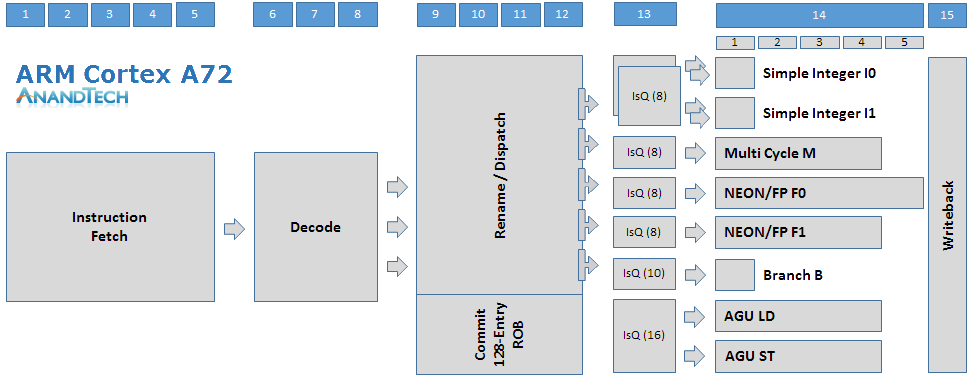
The Cortex A72 is a 15+ stage OoO-pipeline design with a 128 bit fetch and 3-wide decode stage on the instruction-side. Decoding up to 3 instructions into micro-operations (µops) these are then fed into the rename/dispatch stages. The dispatch unit can dispatch up to 5 µops per cycle that feed up to 7 issue queues which in turn schedule µops into 8 execution pipelines.
We find two simple ALUs capable of basic operations such as additions and shifting. Integer multiplication, division and multiply-accumulate operations are handled by a dedicated multi-cycle integer pipeline. Floating point as well as ASIMD and NEON operations are handled by two pipelines, some of the capabilities we’ll go into detail later on. We find a single branch monitor and two dedicated Load and Store AGUs.
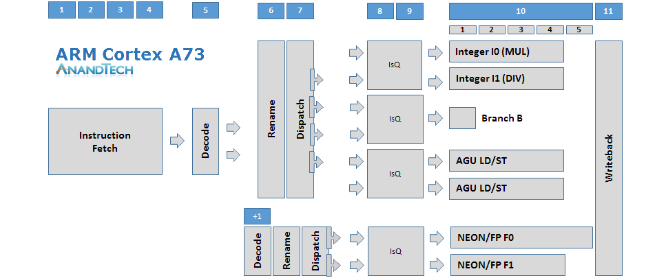
The Cortex A73 looks very similar to the Cortex A17, which in turn is quite different from ARM’s current Austin family of 3-wide decode microarchitectures. The microarchitecture has fundamentally shorter pipeline stages, mostly due to optimizations on the in-order front-end. The fetch stage is only 4 stages deep compared to the 5 stages on the A72. The decode stage is particularly an element which shortens the pipeline length as the A17’s and A73’s decoders are able to decode most instructions in a single cycle as opposed to 3 cycles on the A72. Micro-operations that feed into the floating point pipelines pass through an additional decode stage, making this an 11-12+ deep architecture depending on the type of instructions.
Compared to the A17 the A73 increases its maximum overall dispatch rate from 4 µops to 6 µops. The reservation station for the FP pipeline can still dispatch 2 µops into the common NEON issue queue, the same as on the A17, but the dispatch rate of the integer reservation station has been increased to up to 4 µops, up from 2 on the A17. The dispatch here can feed up to 2 µops for each of the 3 issue queues.
We still have two FP pipelines, and the A73 actually doesn’t change much from the A72 in terms of their capabilities as the A72 had borrowed the A73’s new design. There’s again a single branch monitor, however the AGUs, again like on the A17, are both capable of load and store operations as opposed to the dedicated units found on the A72. Finally on the integer pipelines we see the capabilities of the multi-cycle integer pipeline dissolved into two more complex ALUs. One ALU is capable of multiplication while the other one has integer divide capabilities, all on top of their basic addition and shifter duties. Multiply-accumulate is no longer dedicated and requires execution on both ALUs in tandem.
As the A73 is based off the A17 it continues that microarchitecture’s philosophy: Optimizing the pipeline, resource and interface to achieve the best possible performance at the least possible power consumption while targeting mobile workloads. ARM states that it has especially paid lots of attention to the balance between AArch32 and AArch64 ARMv8 states of the microarchitecture so to that neither is in a disadvantage in either performance or power.
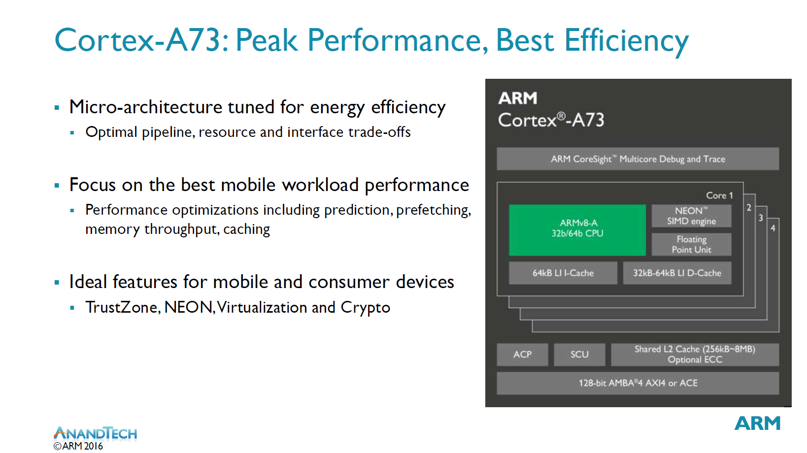
At the cluster level the A73 continues ARM’s quad-core strategy so we are able to use 1 to 4 cores per cluster. The Snoop Coherency Unit (SCU) enables coherency between the cores in a cluster. The L2 cluster is configurable up to 8MB – the same as the A17 and double the amount the A72 supports. ARM still envisions that most vendors will choose to use configurations of 1 to 2MB in consumer products. The L2 cache is inclusive of the L1 cache.
The Accelerated Coherency Port (ACP) is optional and can be left out for mobile designs. The ACP is used for attaching accelerator blocks which are then coherent with the CPU cores and can also make use of the L2 cache. Traditionally this has been mainly something targeted at networking use-cases which weren't as relevant in the mobile space, however ARM sees future potential in machine-learning and computer vision where specialized accelerators can bring tangible performance benefits to a platform.
As opposed to the A15/57/72 who also targeted industrial and large-scale systems, the A73 is mainly targeting the consumer market. Consequently, it drops support the AMBA 5 Coherent Hub Interface (CHI) standard and instead only runs the AMBA 4 ACE (Accelerated Coherency Extensions) standard via a bi-directional 128bit interface. This saves on area and complexity of the microarchitecture's interface. Currently all ARM Cortex big.LITTLE SoCs use ACE interfaces to connect to coherent interconnects such as the CCI-400. Another effect of the design not targeting industrial applications is the lack of support of ECC on the L1 caches, however the L2 can be configured with the feature.

Going deeper into the microarchitecture improvements of Artemis, we start on the instruction side. The I-side on the A73 has been designed to sustain maximum throughput to the rest of the core, as this is one of the most important aspects of a microarchitecture to be able to achieve the best possible IPC. At the same time ARM had to work within set constraints to be able to maintain power consumption.
ARM calls the A17 and A73 “slot-based microarchitectures” which is related to the way the resources are handled and shared among the different blocks of the µarch. As ARM explains it, the A73 sports 8 “slots” where each slot can independently handle all resources on the instruction side. The main advantage of this is that each slot can retrieve information from previous slots in cases of small loops, and thus able to eliminate redundant access to resources on the I-side of the pipeline, a design which is optimal for power consumption. Each slot is given large resources to attain maximum performance, however ARM didn’t want to go into too much detail on this part of the µarch.
The L1 instruction cache 4-way associative and is fixed at 64KB. This is an upgrade over the 32/64KB configuration options on the A17 and also higher than the 48KB that the A72 sports. The upgrade in the L1I cache is a key aspect of the performance improvements of the A73. ARM states that it spent a lot of time optimizing the I-cache for performance and power. One example of this was the way the cache is accessed; if an access is performed but the requesting resource no longer needs the data, the access can be killed on-the-fly to be able to save power.
The instruction fetch block has been optimized to increase maximum throughput to the rest of the core. One optimization was a focus on the removal of “bubbles” for higher IPC. In previous microarchitectures even if a prediction was correct and the I-side was able to send maximum throughput to the decode stage, one could still encounter bubbles as soon as the instruction hit the decode stage it split into micro-operations which introduced them. The A73 detects such cases earlier and is able to send µops directly to the decode stage, resulting in what ARM states in an almost practical elimination of bubbles.
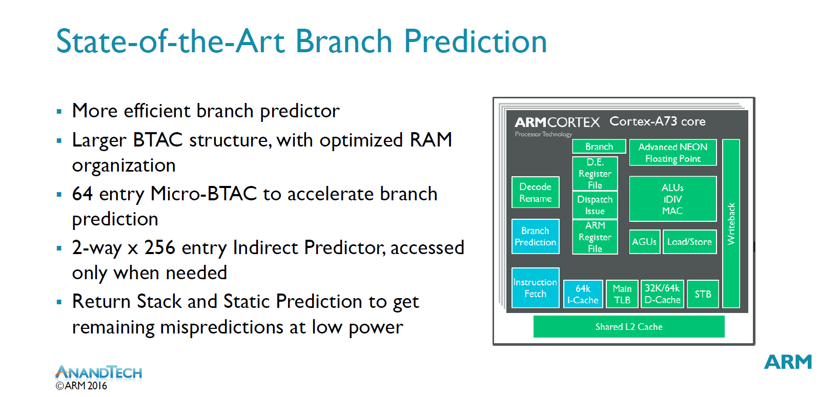
The A73 uses a new “state-of-the-art” branch predictor with very accurate branch prediction. The A73 claims to have a larger BTAC (Branch Target Address Cache) structure, however we unfortunately don’t have any concrete figures on how this has improved. We see the introduction of a new 64-entry “micro-BTAC” which is used to accelerate branch prediction. These two main units are claimed to be able to predict almost all branches.
For the remaining mispredictions the µarch disposes of a static branch predictor and a return stack which is a stack of nested subroutine return addresses. The indirect predictor seems to be an addition when compared to the A17’s branch prediction design, however it's not clear how this 2-way x 256-entry indirect predictor compares or if it differs to the one on the A72.
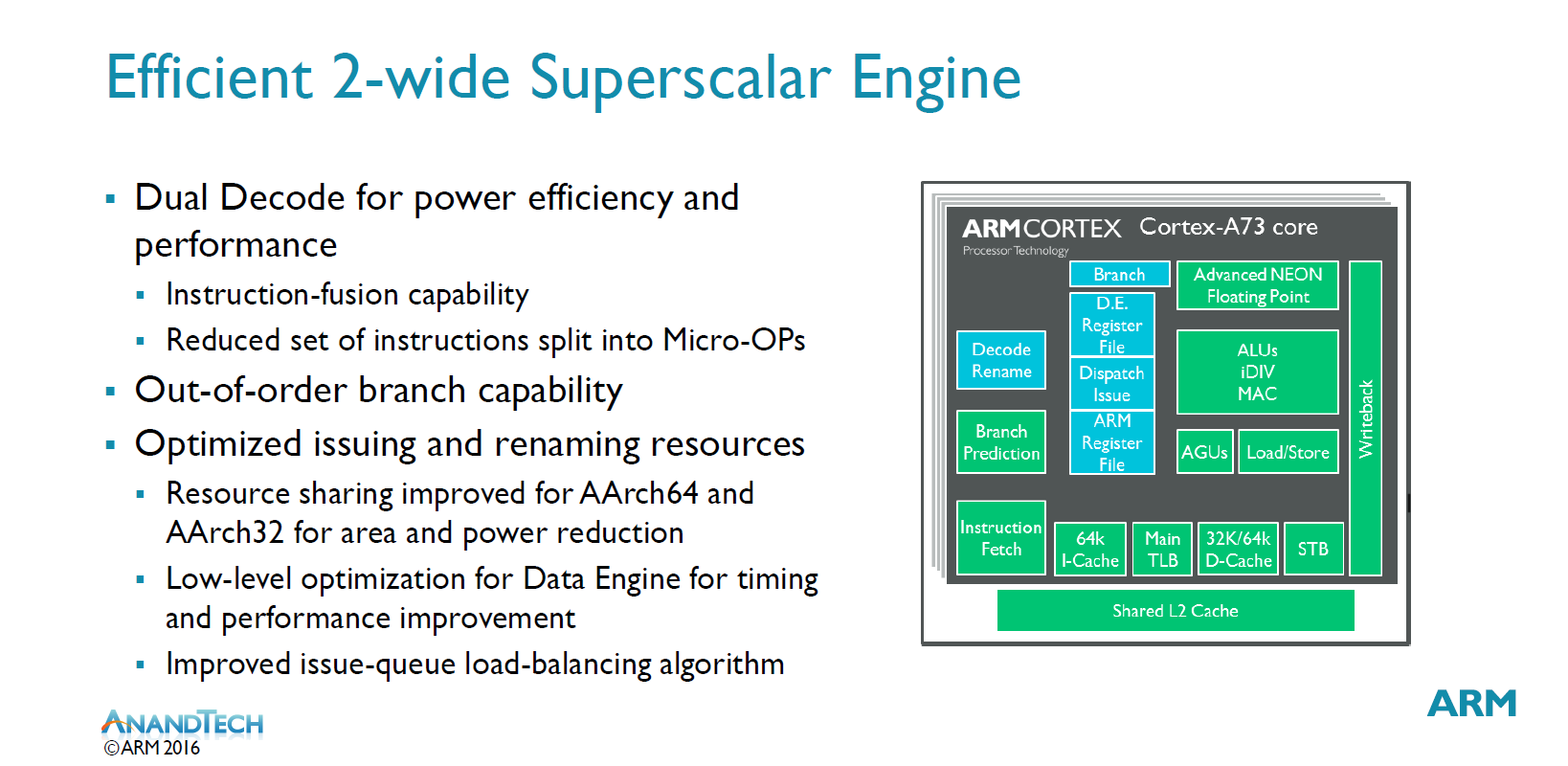
ARM is confident in its ability to increase performance of a 2-wide core while keeping or improving its efficiency. Power is only active to logic that is working on the current “set” of resources. The decoder has seen improvements in its capability to fuse instructions together. Instruction fusion for common idioms is critical for overall performance, but it’s rough to detect them. The A73 pushes further pushes its detection of such idioms through help of former events and is able to detect specific sequences with help of information alongside the whole pipeline.
Splitting instructions into more µops can be helpful for timing reasons, however it also reduces your overall IPC. The A73 reduces the set of instructions which are split into µops to be able to improve on this aspect of the decoder performance.
As mentioned earlier in the overview diagram, the decoder stage is extremely aggressive and is able to decode most instructions in just 1 cycle as opposed to the 3 cycles the A72 µarch family takes. Micro-operations feeding into the ASIMD/NEON pipelines go through an additional decode stage. ARM says that dual load/store units (as opposed to dedicated load and store units) were important to achieving this 1-2 cycle decode capability.
Dispatch rate has been improved over the A17 and now the integer part of the reservation stations can dispatch up to 4 µops into the 3 issue queues (2 µops per IQ) serving the ALUs, AGUs and branch monitor.
An important divergance from the A15/57/72 microarchitectures is the use of a physical register file instead of an architectural one. The benefits of this are a simplification around the rename stage which allow for power savings with high performance. Much like on the A17 this allows for a theoretical "unlimited OoO window", although there are still real limits to it, it does eliminate instruction window bottlenecks for some cases. ARM calls this a "major philosophical change in Out-of-Order micro-architecture approach".
The A73 focuses on optimizing resources from the rename stage up to the issue-queues. The OoO policies on which the issue-queues run on can have a large impact on performance, so special care has been taken to dispatch to the most effective issue-queue. Arbitration in the queues can change on the fly depending on various events, for example when it’s detected that you are in a stream it’s better to issue all store operations in order to be able to deal with a full cache line when feeding the memory system.
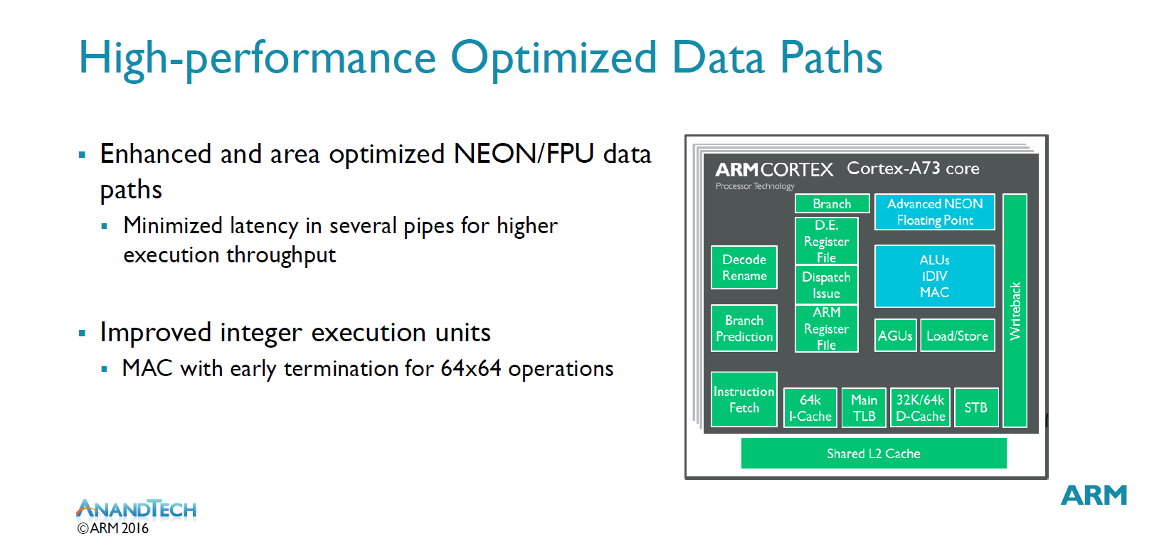
On the data-side when talking about execution pipelines, we don’t see as many improvements as the A73 largely inherits the same NEON units which was introduced on the A72. At last year's TechDay A72 launch we remember ARM stating the new NEON units were brought forward from an advanced future microarchitecture. At the time I had expected this to mean the microarchitecture following the A72, however now ARM unexpectedly tells us that this is a microarchitecture even later than that of the A73. The pulling forward of the NEON units to the A72 is said to have resulted in a lot of learning for the design teams so that we'll actually see even more improvements in the generation following the A73 and even the generation following that. An example of such improvements on the A73 are to be found in miscellaneous FP instructions such as FP transfers and FP moves losing a cycle in some instruction groups. The new NEON units have also seen optimizations to their area usage, making them smaller than in the A72.
The main difference to the A72 lies in the integer units. Instead of 2 basic ALUs with a complex multi-cycle ALU, the A73 sees the latter's capabilities merged into two “beefier” ALUs. Their capabilities isn’t identical: There’s still only one unit which can do division while the other handles multiplication operations. Multiply accumulate operations require both pipelines so this is an degradation compared to the A72 which dedicated such µops to the M pipeline while the two other simple ALUs were free to do other work. The change however also has positive effects as µops for saturating and parallel arithmetic and some miscellaneous data-processing instructions benefit from a doubling in maximum execution throughput.
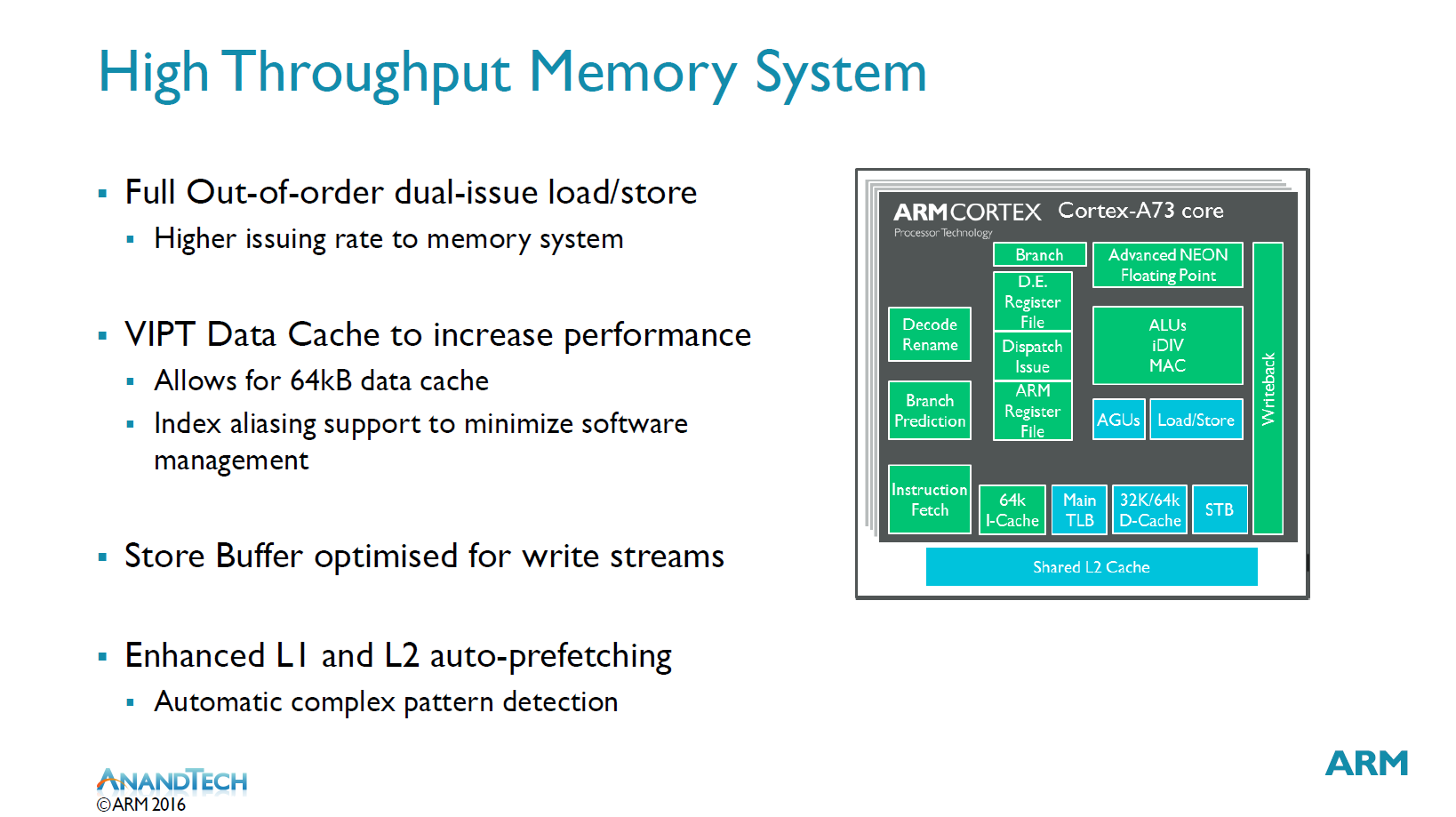
More important than any of the previous aspects of a microarchitecture is the memory system. Again the dual-issue load/store units play a big role in enabling a higher issuing rate into the memory system. The data cache has switched from a PIPT (Physical Index Physical Tag) to a VIPT (Virtual Address Physical Tag) address translation. In a PIPT implementation the largest encountered problem was the translation of addresses to produce indexes, which is one most critical paths of the CPU core. VIPT does away with this problem and also allows for an extended 64KB data cache, up from 32KB on the A17 and A72. ARM claims the larger cache brings an overall 4% performance uplift compared to 32KB. 64KB is the default D-cache size on the A73. Usually software needs to deal with aliasing issues when using VIPT, however the A73 is able to do this in hardware. In hardware the cache is implemented with 4-way associativity but the software sees it as a PIPT 8-way 32kB or 16-way 64KB cache.
A lot of time has been spent on improving the L1 and L2 prefetchers which are large stride based and meant to increase stream performance. Furthermore for irregular patterns there’s the use of an additional prefetcher specialized for the task. ARM is very happy with streaming performance as it’s able to reach near maximum theoretical achievable bandwidth.
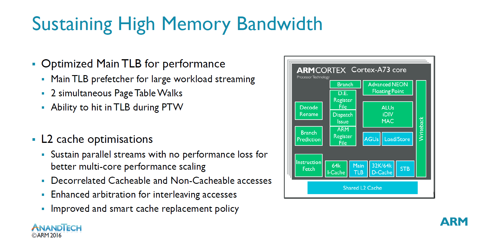
To sustain the improved memory bandwidth there’s also been improvements to the main TLB. In previous microarchitectures large datasets caused performance drops when having to switch to the main TLB. The A73 resolves this issue by giving the main TLB its own prefetchers which allows for sustainable streaming performance even for large data-sets.
On the L2 ARM also improved the resource sharing between CPUs in a cluster. Each CPU has its own dedicated resources so that 1 core streaming will not starve other cores, which enables for parallel streams without performance loss.
Overall in terms of microarchitecture ARM tried to squeeze out the most which is possible out of a 2-wide microarchitecture. We went over what seemed to be some much welcomed improvements to the microarchitecture, but we still need to put it all into context with some performance numbers.
Performance, Power, Area (PPA)
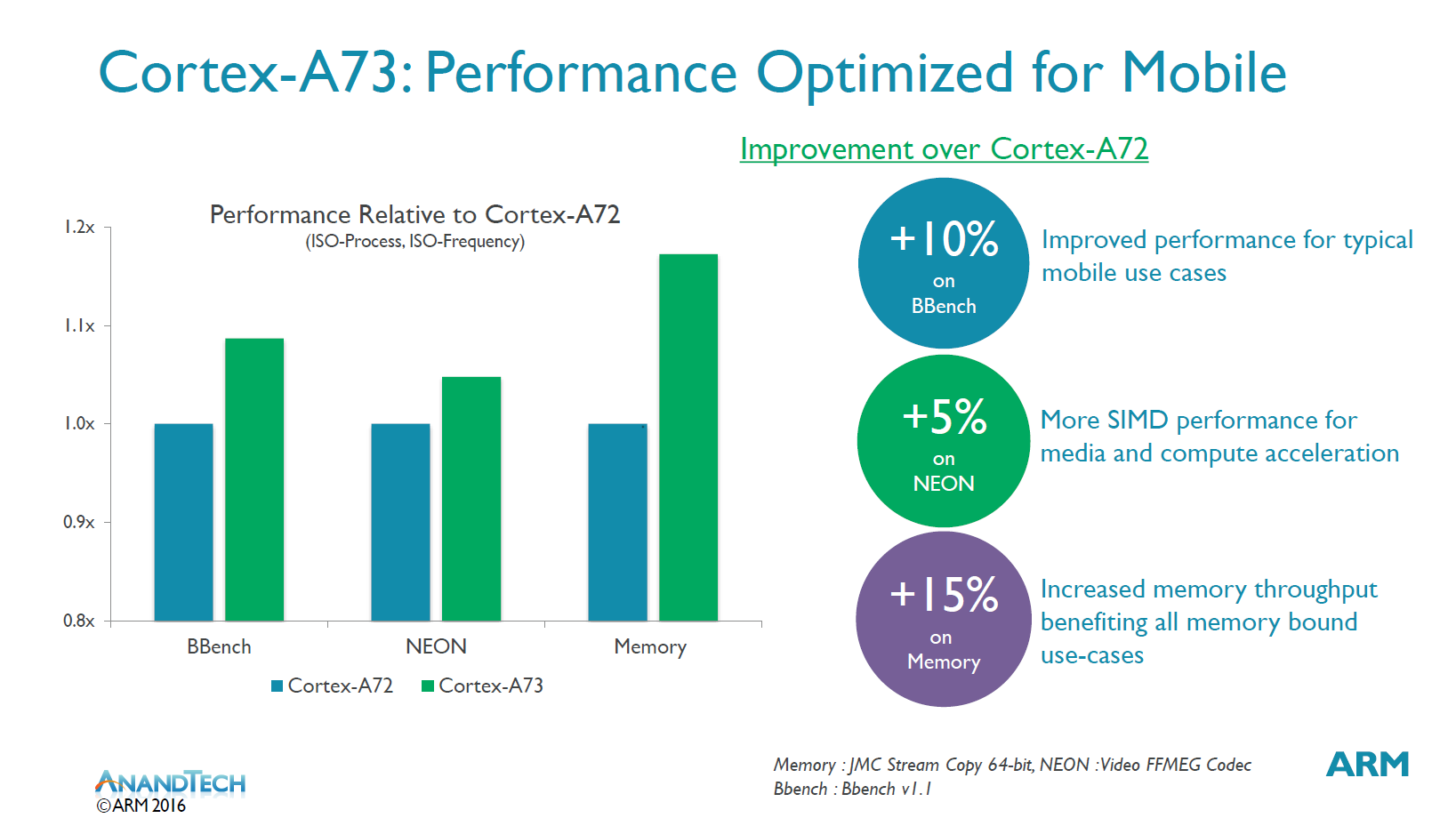
In terms of performance ARM claims it will exceed the A72 in all important metrics relevant to mobile workloads. Examples were scarce but on workloads such as BBench (Website loading benchmark) the A73 is claimed to be up to 10% better performance than the A72 – on the same process and frequency. SIMD/NEON (FFMEG Codec) workloads are supposed to improve by up to 5%, mostly a side-effect from the better memory subsystem. Memory sees the largest gains with up to 15% improvement (JMC Stream Copy 64b).
I asked what we should be expecting in terms of performance degradations and of course the biggest disadvantage will be in micro-benchmarks such as Dhrystone. ARM promises SPEC performance will be the same as on the A72 it’s likely that the downgrade from a 3-wide decoder to a 2-wide one won’t affect many relevant workloads. I saw the same behaviour reflected in the A17 versus the A15 comparison as the former was more than able to keep up with the larger microarchitecture in almost all of the workloads and benchmarks I threw at it, so I have little doubt that the A73 will be able show similar behaviour against the A72.
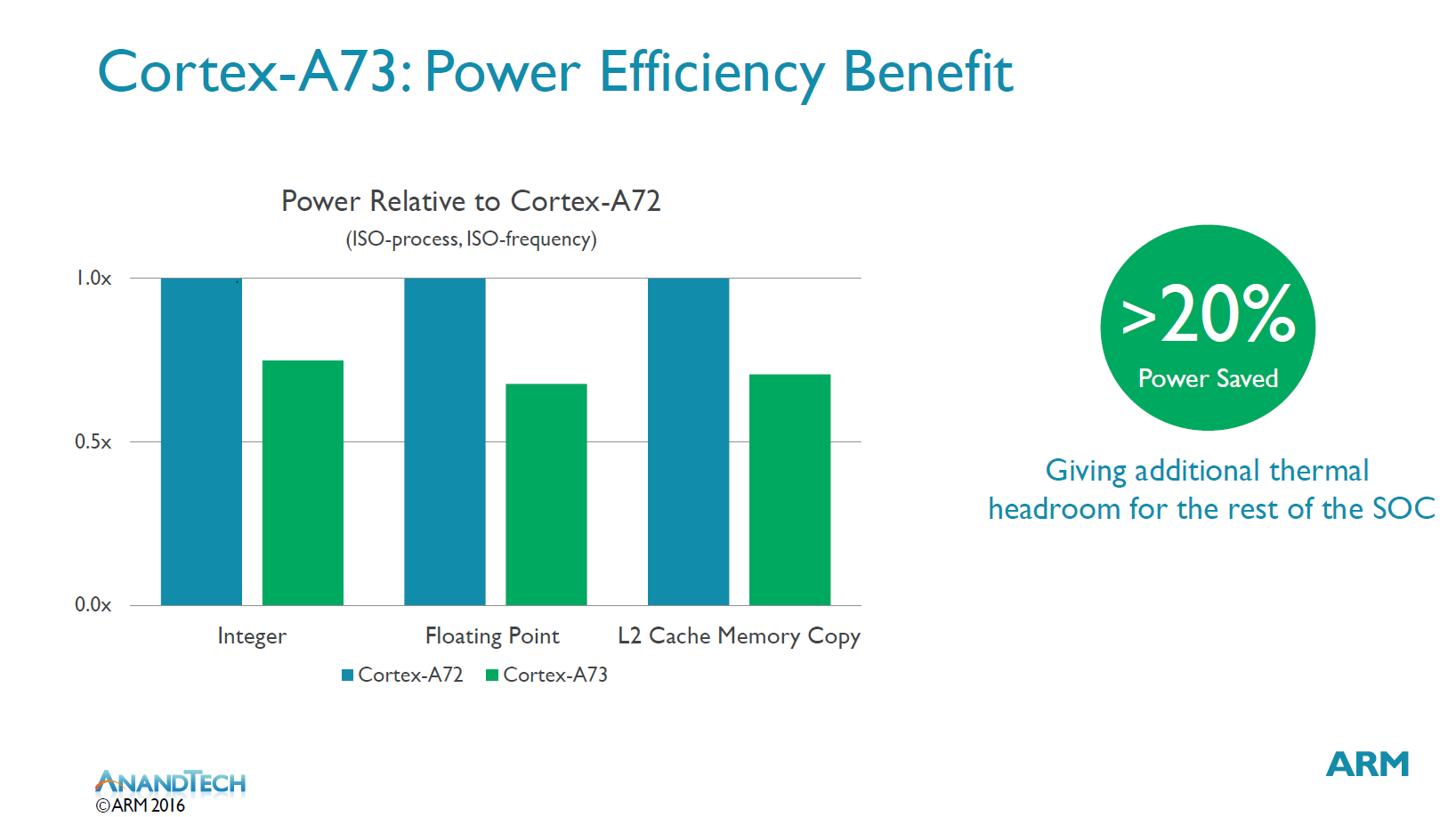
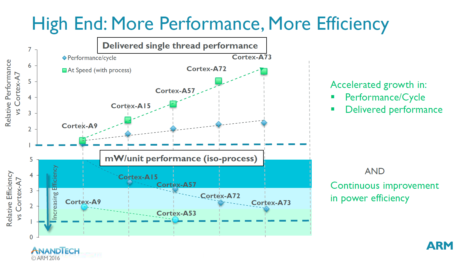
More importantly it’s power consumption which sees the largest improvements. We see up to 25% power reduction in integer workloads and up to ~30% in floating point and L2 cache memory operations. ARM publishes that the A73 uses at least 20% less power than the A72 at the same process and frequency.
An important addition to power efficiency is the inclusion of hardware-governed retention states. This feature was first introduced in the Cortex A35 late last year and now sees adoption in the A73 microarchitecture. Retention is a microarchitectural clock-gating state that was available for a while now, however it was still software controlled, meaning it still had fairly low granularity and most vendors never chose to implement or expose it to current devices as they preferred to fall back to WFI clock gating and power gating. The addition of a hardware governor greatly improves the capabilities of the retention state power management and ARM says that it can bring very significant reductions in dynamic power consumption.

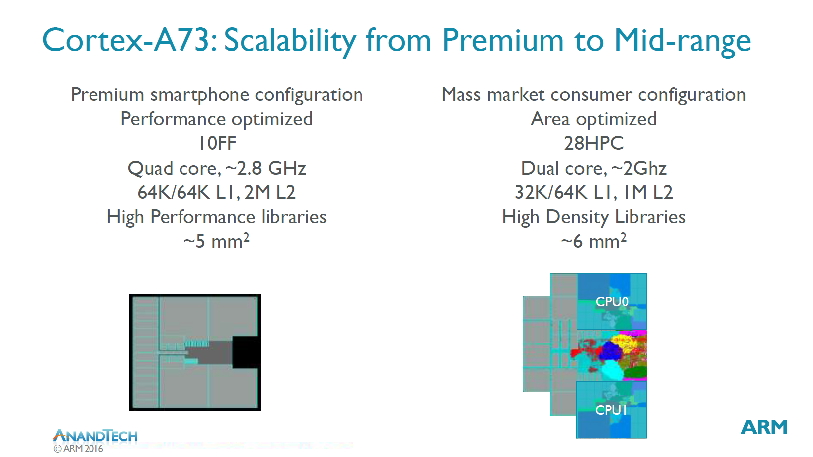
The A73 is up to 25% smaller than the A72 when implemented on the same process with the same performance targets. The A72 is already getting quite small on new process nodes so the A73 will seem quite tiny on future nodes such as 10nm.
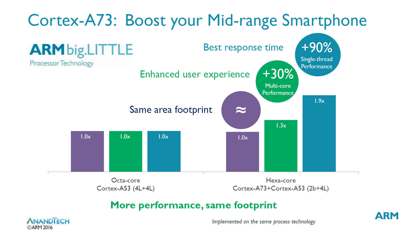
Where the die size reduction will have the biggest impact however is on the mid-range. A 2-core Artemis cluster is supposed to be as big as a 4-core A53 cluster. We’ve seen a lot of 4+4 A53 implementation from various vendors and frankly the performance was not all that convincing as even high-clocked A53’s lagged a lot behind SoCs implementing big high-performance microarchitectures. It’s only been recently with the Snapdragon 650 and 652 that we’ve finally see performance of the mid-range catch up to that of more expensive flagships. ARM makes a point for replacing these 4+4 A53 SoCs with 2+4 A73+A53 SoCs as they’re able to keep the same area footprint (which in terms means same cost for the vendors) while vastly improving single-thread performance.
While vendors will certainly be able to use the A73 on older process nodes such as 28nm, ARM talked more about future nodes such as 10nm. Here again we see ARM aiming for low power and sustained performance and says we’ll see clock of up to 2.8GHz under a 750mW power budget (SPEC2K workload). This seems a rather conservative figure and I’m not sure if vendors will follow ARM’s guidance here – it’s more likely we’ll see SoCs try to hit and go over 3GHz on 10nm while the 2.8GHz target seems perfectly doable on 16nm. Of course this all depends on if the vendors are able to do a physical implementation that is close to ARM’s POP results, such as HiSilicon’s Kirin 950.
Closing Thoughts
Overall ARM’s decisions with the A73 make a lot of sense. ARM's big cores definitely needed to improve in terms of power and efficiency. A72 was a first step towards that goal and A73 further improves in that regard. In the future we should expect ARM to eventually again return to wider microarchitectures as we hit the wall of diminishing returns in terms of frequency scaling. HiSilicon's Kirin 950 was a game-changer in terms of perception and analysis of ARM’s microarchitectures as we finally have a vendor that was able to hit power figures near those that ARM publishes, lending the latter much more credibility when talking about efficiency goals.
If the A73 is able to hit all of its promised targets then it leaves me with some doubt on what this means for vendors who are currently using their own microarchitectures. Apple has proven that they’re able to execute and deliver outstanding performance at high efficiency, but vendors such as Qualcomm and Samsung aren’t in an as good position. We'll have a more in depth discussion about Snapdragon 820’s Kryo and Exynos 8890’s Mongoose cores in an upcoming deep dive article, but both microarchitectures have trouble in terms of differentiating themselves in terms of performance and power compared to ARM’s own current designs, casting some doubt on how they'll be able to evolve and compete against SoCs using Artemis cores.
ARM states that we’ll be seeing SoCs and actual consumer devices with A73 by the end of the year. This would mark the second year in a row where vendors would be ship within less than a year from announcement of a new ARM microarchitecture, and given the stated release schedule and looking back at last year’s SoCs with A72 cores, it shouldn't be too hard to guess which device and chipset might be able to fit this timeline.
All in all, I’m pretty happy with the direction ARM went with in the A73. It addresses a lot of the issues brought up in the introduction, and while more performance is always wanted, efficiency needed to be in focus this generation, and efficiency we got.


